
Samsung has a roadmap taking its chips to 3nm process technology as soon as 2022
Last week, Samsung held its annual Foundry Forum in the U.S. At the event, the company revealed a roadmap that takes its process technology to 7nm Low Power Plus, 5nm Low Power Early and 3nm Gate-All-Around Early/Plus. The 7nm LPP process will be Samsung's first to use an EUV lithography solution, and should be ready for production during the second half of this year. Mass production of parts using the new process will start in the first half of 2019. That happens to be when rival TSMC will start mass production of parts using its 7nm+ node (also using EUV lithography), and start risk production of its 5nm node.
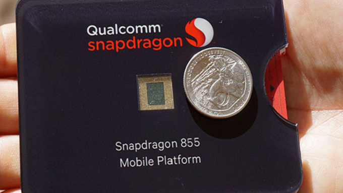
Chips based on Samsung's 5nm LPE will provide ultra-low power consumption. And the last of the chips to employ FinFET will be produced using the 4nm Low Power Early/Plus process. Chips built with this process technology will feature improved performance and a smaller cell size. The two will begin production in 2019 and 2020, respectively. Earlier this year, we passed along a report out of Korea that said Samsung will produce the 7nm Snapdragon 855 mobile platform, which will reportedly be powering next year's Samsung Galaxy S10.
Starting with the 3nm node, Samsung will use its own next-generation GAA (Gate all-around) architecture MBCFET (multi-bridge-channel FET). 3nm production is not expected to begin until 2022. Keep in mind that the smaller the node size, chips that are produced using the process are more powerful and energy efficient.
source: Digitimes
Follow us on Google News


![Some T-Mobile users might be paying more starting in March [UPDATED]](https://m-cdn.phonearena.com/images/article/176781-wide-two_350/Some-T-Mobile-users-might-be-paying-more-starting-in-March-UPDATED.webp)


Things that are NOT allowed:
To help keep our community safe and free from spam, we apply temporary limits to newly created accounts: