China introduces its first domestically made e-beam lithography machine
Has China found a solution to get around U.S. sanctions on EUV lithography machines.

We've often said that the inability of Chinese foundries and tech manufacturers to obtain Extreme Ultraviolet (EUV) lithography machines is the big reason why China is so far behind in the chips race. Thanks to U.S. and Dutch officials, the one company that makes advanced lithography gear, Dutch firm ASML, cannot ship the latest EUV lithography equipment to China. However, less advanced Deep Ultraviolet (DUV) lithography machines, using older technology, can still be shipped to China.
This is important because EUV machines are needed to manufacture chips under 7nm. Foundries like TSMC and Samsung Foundry will be mass producing chips using their 2nm process nodes this year. Lower process node numbers mean that the transistors used are smaller, allowing more to fit into a small space inside a chip. This number is called the Transistor Density and is usually shown as millions or billions of transistors per square millimeter. The higher the transistor density, the more powerful and energy-efficient a chip is.
China might have a chip-making breakthrough with the debut of a homegrown e-beam lithography machine
The lithography machine is used to transfer circuitry patterns onto the silicon wafers that serve as the foundation of the chips manufactured by foundries. Deep Ultraviolet (DUV) light has a wavelength of 193 nanometers. EUV, however, uses light with a wavelength of just 13.5 nanometers, which is about 14 times shorter. This shorter wavelength allows EUVs to etch the fine patterns needed for today's intricate chip designs.
"Due to export controls, such equipment has long been out of reach for leading domestic research institutions, including the University of Science and Technology of China and Zhejiang Lab."
-Hangzhou Daily
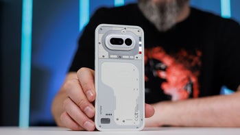
But the Chinese have built their first e-beam lithography machine, which they have titled Xizhi. It was created at Zhejiang University in Hangzhou and uses focused electron beams to etch the circuitry patterns on the silicon wafers. The downside is that e-beam lithography cannot produce chips at a large scale like DUV and EUV machines can. But for China, it's any port in a storm when it comes to lithography, and the e-beam lithography works great during the testing phase of production.
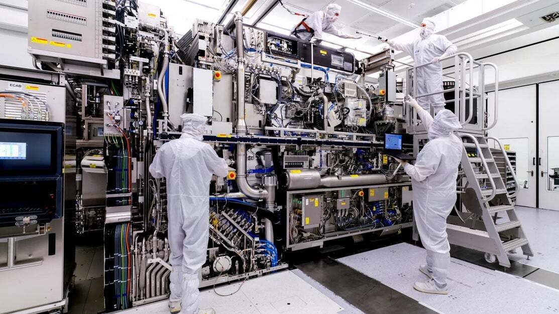
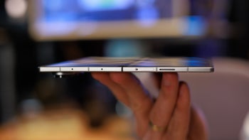
An ASML built Extreme Ultraviolet lithography machine. | Image credit-ASML
A local newspaper, Hangzhou Daily, said on Thursday, "Due to export controls, such equipment has long been out of reach for leading domestic research institutions, including the University of Science and Technology of China and Zhejiang Lab. The delivery of Xizhi is expected to help break this impasse." Xizhi can etch circuit lines as narrow as 8 nm, with a positioning accuracy of 0.6nm. This meets international standards.
Will e-beam lithography help Huawei's phones compete with Apple, Samsung?
Yes. This is big news for Huawei.
41.78%
No. This is not an advanced lithography replacement.
21.92%
Too early to make a call.
36.3%
Discussions with Chinese companies and research institutes interested in Xizhi have begun. The domestically produced e-beam lithography machine is cheaper than similar devices imported into China. This is just the beginning of China's attempt to bypass U.S. restrictions by producing its own chipmaking equipment. There are reports that Huawei has been working on building its own EUV machine.
Huawei is reportedly testing its own EUV lithography machine
Reportedly, Huawei has been testing a trial EUV machine at its factory in Dongguan. Supposedly, Huawei will aim for trial production later this year with mass production expected to take place in 2026. Should Huawei be able to create an EUV machine, it would be a big deal for China in general and Huawei in particular. It could allow Huawei and China's largest foundry, SMIC, to produce cutting-edge chips that might be able to compete with the silicon designed by U.S. chip design heavyweights like Apple, Qualcomm, and Nvidia.
Before the U.S. implemented the sanctions preventing Huawei from obtaining cutting-edge chips, the Chinese manufacturer's HiSillicon chip design unit was TSMC's second-largest customer after Apple. At that time, HiSilicon and thus Huawei had access to TSMC's most cutting-edge process nodes. In fact, the last chip TSMC produced for HiSilicon before U.S. sanctions kicked in was the Kirin 9000 AP. Built using TSMC's 5nm process node, this was the SoC used to power the Huawei Mate 40 series in 2020.
After the sanctions went into effect, Qualcomm was given a license from the U.S. Commerce Department allowing it to ship 4G Snapdragon chips to Huawei. In 2023, Huawei stunned the industry by releasing the Mate 60 series powered by the Kirin 9000S. Produced by SMIC, the SoC was built using the foundry's 7nm process node and brought 5G support back to Huawei's flagship phones.

Popular stories


Latest News


Things that are NOT allowed:
To help keep our community safe and free from spam, we apply temporary limits to newly created accounts: