
Huawei says it has unconventional way to produce advanced 1.4 nm chips for its devices
Huawei will use an unconventional method to build advanced chips by 2031.

Huawei devises new way to make advanced chips | Image by PhoneArena
As you might remember, Huawei was placed on the U.S. Entity List in 2019 preventing it from accessing its U.S. supply chain. The following year, the U.S. made matters worse by using the Foreign Direct Product Rule (FDPR) to prevent Huawei from obtaining cutting-edge chips from foundries that use U.S. software and equipment to manufacture these components.
Why Huawei can't obtain cutting-edge chips
The two major foundries producing chips using advanced process nodes both rely on American-made equipment and software. As a result, Huawei could not have its chips, designed by its HiSilicon unit, manufactured with the same high transistor density and transistor count as those produced by TSMC and Samsung Foundry. Chips with a high transistor density often have a high transistor count making them powerful and energy efficient.
At first, Huawei received approval to use special versions of Qualcomm's Snapdragon application processors (APs) that were modified to work with 4G networks, not 5G networks. These are the flagship phones that used this workaround:
2021
- Huawei P50-Snapdragon 888 4G
- Huawei P50 Pro-Snapdragon 888 4G
2022
- Huawei Mate 50-Snapdragon 8+ Gen 1 4G
- Huawei Mate 50 Pro-Snapdragon 8+ Gen 1 4G
2023
- Huawei P60-Snapdragon 8+ Gen 1 4G
- Huawei P60 Pro-Snapdragon 8+ Gen 1 4G
- Huawei Mate X3-Snapdragon 8+ Gen 1 4G
For the Huawei Mate 60 flagship series, the company wanted to offer 5G on its phones once again. So it designed a new Kirin chip and turned to China's largest foundry, SMIC, to build it. However, U.S. sanctions prevented SMIC from obtaining advanced lithography equipment from the one company in the world that makes the extreme ultraviolet (EUV) lithography machine.
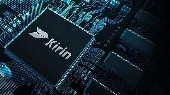
Since late 2023, Huawei has returned to equipping flagships and foldable phones with its own Kirin processors. | Image by Huawei
These machines transfer circuitry designs on the silicon wafers that chips are built on. The 13.5nm EUV wavelengths allow much thinner lines to be printed on the wafers allowing for higher transistor density. SMIC was allowed to own the previous generation of lithography machines called Deep Ultraviolet lithography, which features wavelengths of 193nm.
In 2023, Huawei produced its first 5G flagship phone since 2020
Who will this new chip designing process hurt the most?
83 Votes
TSMC and Samsung Foundries.
38.55%
Apple, Samsung, and Google
25.3%
Other Chinese phone manufacturers.
10.84%
No one.
25.3%
Using multiple patterning, a circuit design is printed two or more times on a wafer to make up for the limits imposed by using a DUV lithography machine. Even using this process, Huawei was limited to using a 7nm chip for the Mate 60 Pro while Apple was using a 3nm A17 Pro AP for the iPhone 15 Pro and iPhone 15 Pro Max. But for the first time since 2020, Huawei was able to sell a flagship with 5G support out of the box in 2023.
Why Huawei had to move away from traditional chip design
Huawei will be able to start producing advanced Kirin chips by 2031 thanks to a new chip design it announced today. Instead of making transistors smaller allowing more of them to fit inside a chip, Huawei will make chips more powerful through improved chip design. Huawei has to look at alternatives to traditional chip design because it seems unlikely that the U.S. will ever drop the sanctions on Huawei when it comes to foundries and lithography machines.
Huawei says that it will be able to design chips by 2031 that will have a transistor density equivalent to a 1.4nm chip. TSMC will start mass production of 1.4nm chips by the second half of 2028. While Huawei will still be behind by 2031, it will have closed the gap with leading foundries dramatically.
Huawei's concept was presented Monday at the 2026 IEEE International Symposium on Circuits and Systems
The concept was presented by He Tingbo, president of Huawei's semiconductor business during a keynote speech at the 2026 IEEE International Symposium on Circuits and Systems (ISCAS) in Shanghai on Monday. The Tau Scaling Law reduces the time it takes signals and data to move through chips and computing systems.
Huawei says that it has already used the Tau Scaling Law on 381 chips over the past six years. These chips were used for the smartphone and AI computing industries. Starting this fall Huawei will use LogicFolding, a related architecture that shortens wiring inside chips, to improve performance on Kirin chips.
Huawei has tried other ways to get around the U.S. sanctions including patenting its own advanced lithography machines. But so far it doesn't appear to have been able to move forward in this direction. The Tau Scaling Law seems to have potential and appears to be Huawei's best shot to obtain advanced process node chips.


Popular stories




Latest News




Things that are NOT allowed:
To help keep our community safe and free from spam, we apply temporary limits to newly created accounts: