TSMC's A16 process node will be ready for mass production later this year
Later this year TSMC will be ready to start mass production of its next process node.

What TSMC has after the 2nm process node. | Image by TSMC
Trivia time boys and girls. Which smartphone was the first powered by an application processor (AP) made using a 2nm process node? The iPhone 17 Pro Max is not the correct answer as the A19 Pro AP is manufactured by TSMC using its third-generation 3nm node (N3P).
The first smartphone powered by a 2nm chip was released earlier this year
The first smartphones to sport a 2nm AP were the Samsung Galaxy S26 and the Galaxy S26+ in Europe, South Korea, India, Southeast Asia, the Middle East, and Africa. In those markets, the two aforementioned models were powered by the Exynos 2600. The latter is designed by Samsung and is built by Samsung Foundry using its 2nm process node.
The previous year, the Exynos 2500 AP was built using Samsung Foundry's 3nm process node. The lower the process node, the smaller the transistors used in the chip allowing more transistors to be packed inside, increasing transistor density. The density formula is the number of millions of transistors in a chip divided by square millimeters.
Why higher transistor density is so important
Higher density numbers are important because it means that more transistors can fit on a single chip. It also means that electrons have shorter distances to travel hiking clock speeds and allowing tasks to be handled faster by these chips. Denser chips require less power to turn transistors on and off which is why the move to 2nm chips should result in better battery life on some phones.
What material might replace silicon for chips in the future?
Graphene as it conducts electrons 100 times faster.
39.02%
Gallium Nitride
24.39%
Bismuth.
0%
Potatoes (haven't you heard of potato chips?)
7.32%
I have no clue.
29.27%
TSMC's 2nm chips also use Gate-All-Around (GAA) that covers the channel on all four sides, not just three sides like FinFET. As a result, current leaks are greatly reduced and the drive current is increased allowing a transistor to switch between "On" and "Off" states faster. This allows for faster clock speeds and overall processing by the chip.
TSMC will debut its Super Power Rail with the A16 process node
After 2nm, TSMC will begin its Angstrom era of process nodes starting with A16 and continuing with A14, A13, and A12. A16 will feature TSMC's version of Backside Power Delivery, which the Foundry calls Super Power Rail (SPR).
Typically, wires for data and power are connected on the front side of a silicon wafer. SPR moves the wires delivering power to the back of the silicon wafer, directly to the transistor's source and drain. As a result, these wires don't have to make it through as many as 15 layers of wiring which can produce electrical resistance and a drop in voltage.
Additionally, removing the power wires from the front of the wafer allows signal wires to be packed more tightly together increasing transistor density without having to resort to a smaller process node. The shorter and more direct electrical path means that less energy is wasted as heat. It also allows transistors to switch faster, perfect for complex and intensive tasks like generative AI.
This is when mass production using the A16 node will start
Both Intel and Samsung have versions of Backside Power Delivery with Intel's called PowerVia. TSMC will debut SPR with its A16 node. Compared to its enhanced 2nm node (N2P), A16 is expected to deliver an 8%-10% increase in speed at the same voltage, consume 15-20% less power at the same speed, and up to a 10% increase in chip density.
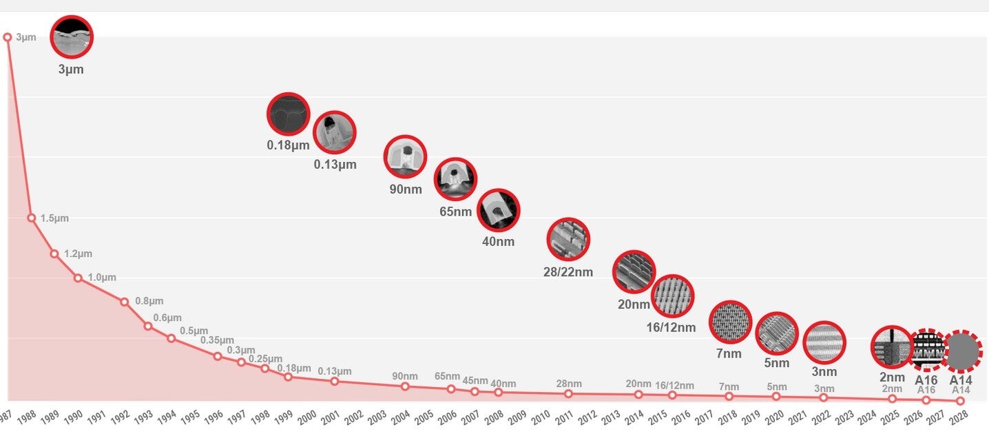
The timeline that took TSMC to its 16A process node. | Image by TSMC
Mass production using the A16 node is expected to start during Q4 2026 although chips using the process node aren't expected to see the light of day until 2027-2028. The A16 will also be known as the N2X. A13, due in 2029, will feature a 6% reduction in area making it useful for HPC (High-Performance Computing), AI, and Mobile.
The reduction in area also means that a single silicon wafer can yield more chips lowering the price per chip. It is backward compatible with the A14 design allowing companies to use existing designs with the smaller node without having to redesign them.
It looks like we shouldn't be worried about the near-term future of the chip industry, at least for the next four to five years.

Popular stories


Latest News


Things that are NOT allowed:
To help keep our community safe and free from spam, we apply temporary limits to newly created accounts: