
Intel video shows the $400 million tool that will help it build more powerful chips

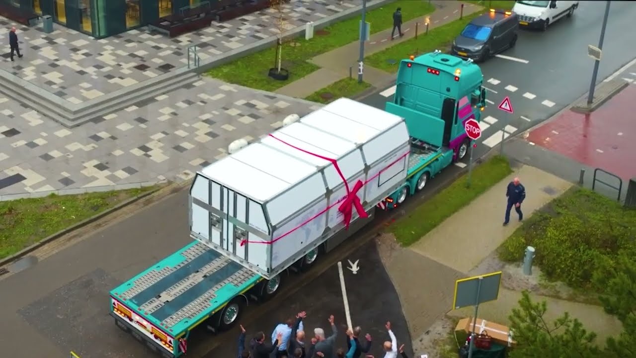
Extreme ultraviolet lithography (EUV) machines are huge, about the size of a school bus. And they are expensive, too. Only one company, Dutch firm ASML, makes the machines which are used to etch circuitry patterns on silicon wafers. As chips get smaller and carry billions of transistors, these patterns have to be thinner than human hair and that's where the EUV machines come in.
The latest generation of EUV machine, known as the High-NA EUV, is expected to be used to help build chips using a 2nm process node and smaller. As we told you back in December, Intel was the first company to purchase the $400 million machine and plans on using it for production of chips using its 18A (18 angstroms) 1.8nm process node starting next year (but not for high-volume production).
Intel will, as it promised more than a couple of years ago, have snatched back process leadership from TSMC and Samsung Foundry. The latter two foundries will be at 2nm by the second half of next year. Still, the main goal for Intel out of the box is to learn how to use the machine flawlessly so that the company will have no issues with high-volume production using its 14A (1.4nm) process node expected to begin in 2027.
The reason that this is so important is that the feature size of a chip shrinks along with the process node number. Smaller transistors mean that more can fit inside a chip and the higher a component's transistor count, the more powerful and/or energy-efficient that chip is. The iPhone 11 line in 2019 was powered by the 7nm A13 Bionic SoC containing 8.5 billion transistors. The 3nm A17 Pro SoC, used to power the 2023 iPhone 15 Pro and iPhone 15 Pro Max, carries 19 billion transistors in each chipset.
Intel's purchase of ASML's Twinscan EXE:5000 High-NA EUV machine was delivered to the company in 250 separate crates that Tom's Hardware says weighed in at 330,000 pounds. While the unit has been installed at Intel's fab, it will take six months of work from 250 ASML and Intel engineers to completely install the High-NA EUV machine. And it could take several weeks or months to calibrate the machine which prints at an 8nm resolution compared to the 13nm resolution that current Low-NA EUV machines print at.
The result? An ability to produce transistors 1.7 times smaller which can triple the transistor density of a chip. ASML says that it has received 10-20 orders for its High-NA EUV from companies such as TSMC, Samsung Foundry, and SK Hynix.

Popular stories


Latest News


Things that are NOT allowed:
To help keep our community safe and free from spam, we apply temporary limits to newly created accounts: