
Apple and Huawei's 2020 flagships should deliver a huge performance boost
2020 is a big year for the mobile chip industry. That's because, in the middle of this year, the world's largest independent foundry, Taiwan Semiconductor Manufacturing Company, Limited (TSMC) will start shipping chips manufactured using the 5nm EUV process. As process numbers drop, the number of transistors inside integrated circuits rise. As an example, the 7nm Apple A13 Bionic chipset contains approximately 8.5 billion transistors. The 5nm A14 Bionic will reportedly employ 15 billion transistors.
As the number of transistors inside chips goes up (theoretically doubling every other year, an observation known as Moore's Law) these components not only become more powerful, they become more energy-efficient as well. As a result, the two major phone manufacturers with access to 5nm chips this year will benefit. Those companies are Apple and Huawei. With the A14 Bionic inside the iPhone 12 series, we should see more powerful iPhone models later this year that could build on the outstanding battery life seen on the iPhone 11 line.
The Huawei Mate 40 series should be powered by the 5nm Kirin 1020 chipset
Turning to Huawei, the company's most technologically advanced flagship phone line of the year will be this fall's Mate 40 series. And the Mate 40 and Mate 40 Pro handsets are expected to be powered by Huawei's next-generation Kirin chipset which has been dubbed the Kirin 1020 for now (with the code name of Baltimore). Like Apple, Huawei designs its own chips (through its HiSilicon unit) and relies on TSMC to manufacture them.
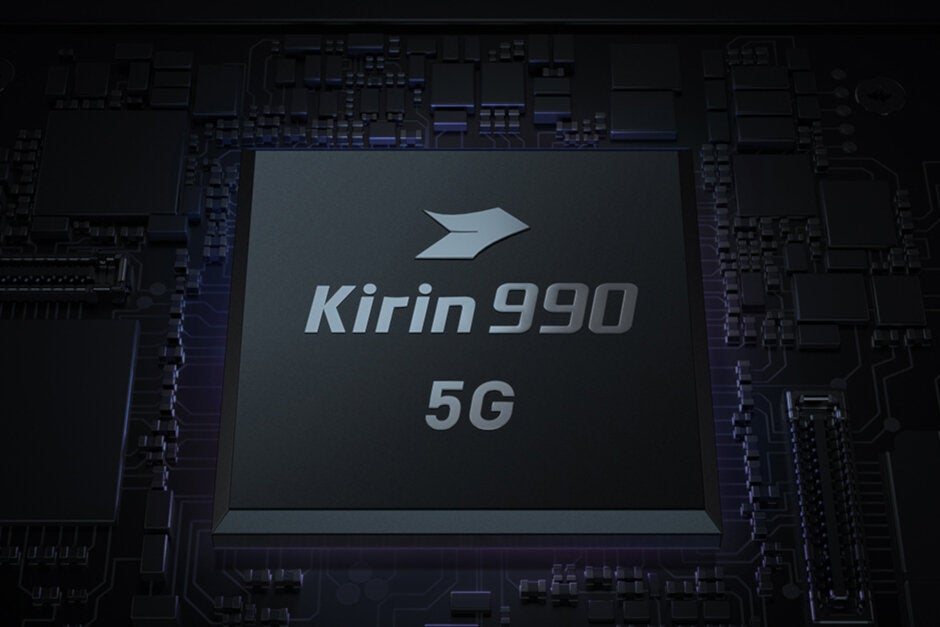
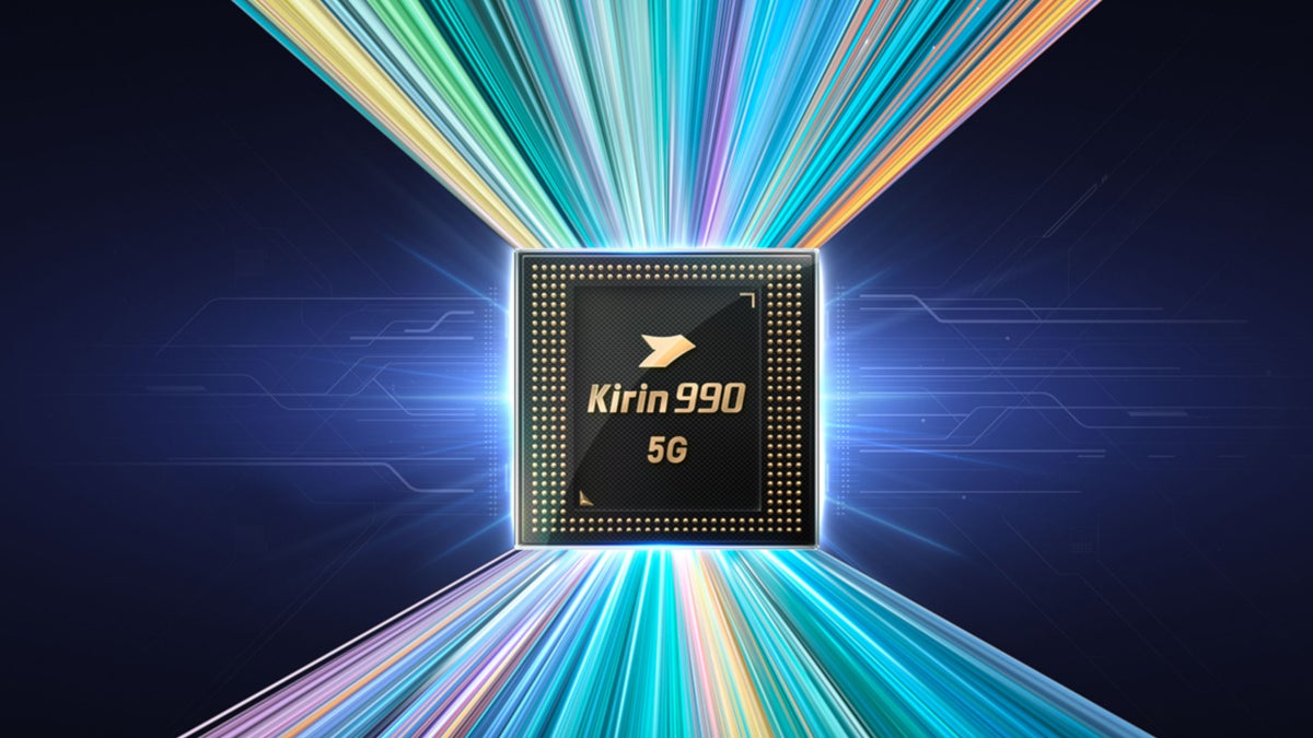
The 7nm Kirin 990 5G is going to power the Huawei P40 and P40 Pro
According to MyDrivers (via WCCFtech), the new 5nm Kirin chip will provide a 15% savings in power consumption compared to the current 7nm Kirin 990 SoC that will be used on the upcoming Huawei P40 line. And if the new chip employs ARM's Cortex-A78 CPU core as rumored, the performance hike over the current chip could reach 50% over the Kirin 990 5G. Speaking of which, a 5G modem will be integrated with the Kirin 1020 SoC. The report also notes that the transistor density on the latter component will increase by 80% from the density seen on the Kirin 990. That figure alone should tell you all you need to know about the amazing strides that have been made and are continuing to be made in the industry every 2-3 years.
Transistor density is measured in transistors per square mm. In 1970, that figure hit 300 while chips were being made using the 8000nm process. Ten years later, the density figure had reached 7,280 transistors per square mm for the 1000nm process. By 2008, chip manufactures were able to squeeze 3.3 million transistors into a square mm as the process node had dropped to 45nm. And the transistor density for 5nm integrated circuits will be 171.3 million per square mm. Many believe that we are coming to the end of Moore's Law but both TSMC and Samsung are working on alternative production techniques to overcome the physical limitations that could prevent the process node from shrinking beyond 1-2nm.
The EUV part of the 5nm EUV process refers to a technology called extreme ultraviolet lithography. With EUV, an ultraviolet beam is used to more precisely mark patterns on a chip die. These patterns relate to the placement of transistors inside a chip. Thanks to the precise patterns created by EUV, more transistors can be stiffed inside a chip. Both TSMC and Samsung have roadmaps that take chip production down to 3nm by 2022-2023.
Since only Apple and Huawei are expected to have access to 5nm chips this year among mobile phone manufacturers, you might be wondering when the majority of Android phones will be equipped with a 5nm chip. TSMC is expected to build the Snapdragon 875 Mobile Platform using the 5nm node and the first phones to be powered by these chips will be released early in 2021.

Popular stories


Latest News


Things that are NOT allowed:
To help keep our community safe and free from spam, we apply temporary limits to newly created accounts: