Intel will bring a performance-improving feature to its chips one year ahead of TSMC
In October 2021, Intel CEO Pat Gelsinger said that Intel would reclaim process leadership from TSMC and Samsung Foundry by 2025. Intel is looking to challenge TSMC and Samsung Foundry in the contract foundry segment of the industry. A contract foundry takes the chip designs from fabless chip designers (fabless means that they do not own a fabrication facility, like Apple for example) and manufacturers the chip. TSMC is the global leader followed by Samsung Foundry.
Currently, both TSMC and Samsung Foundry are shipping 3nm chips and in the second half of next year, both could be mass-producing 2nm chips. Later this year, according to The Motley Fool, Intel will be using its 20A process (equivalent to 2nm for TSMC and Samsung Foundry) which will be used to build Intel's Arrow Lake PC chips. So at that point, Intel will have process leadership and that will only continue next year when Intel debuts its 18A process node, equivalent to 1.8nm when you compare it to TSMC and Samsung Foundry. The latter two will be debuting their 2nm node in the second half of next year.
Intel's process nodes will go from 20A this year to 14A by 2027
Everyone is expected to catch up with each other in 2027 when Intel's 14A (1.4nm) joins 1.4nm output from TSMC and Samsung Foundry. The bottom line is that the size of the transistors used with these chips gets smaller as the process node shrinks. That means more transistors can fit inside a component. The more transistors inside a chip, typically the more powerful and/or energy efficient a chip is.
Intel will debut its 18A process node next year
But starting with its 20A production later this year, Intel will have a bit of a head start on TSMC and Samsung Foundry with a key feature that the American chipmaker calls PowerVia (also known as known as backside power delivery). TSMC is expected to use this technology with its N2P node which it will use starting in 2026. Samsung Foundry is supposedly going to use backside power delivery on a particular node launching next year, although Samsung Foundry has not confirmed this.
So what is PowerVia? Most of the small wires that deliver power to a chip are found on top of all of the layers that make up a silicon component. As these chips become more powerful and complex, the wires on top that connect to power sources are competing with the wires that connect components. This results in wasted power and low efficiency.
PowerVia moves the wires bringing power to the chips to the backside of the chip. As a result, clock speeds can increase by 6% resulting in greater performance. Add to that the increase in performance delivered by using a more advanced process node, and the result is a more powerful chip used to run a more powerful device.
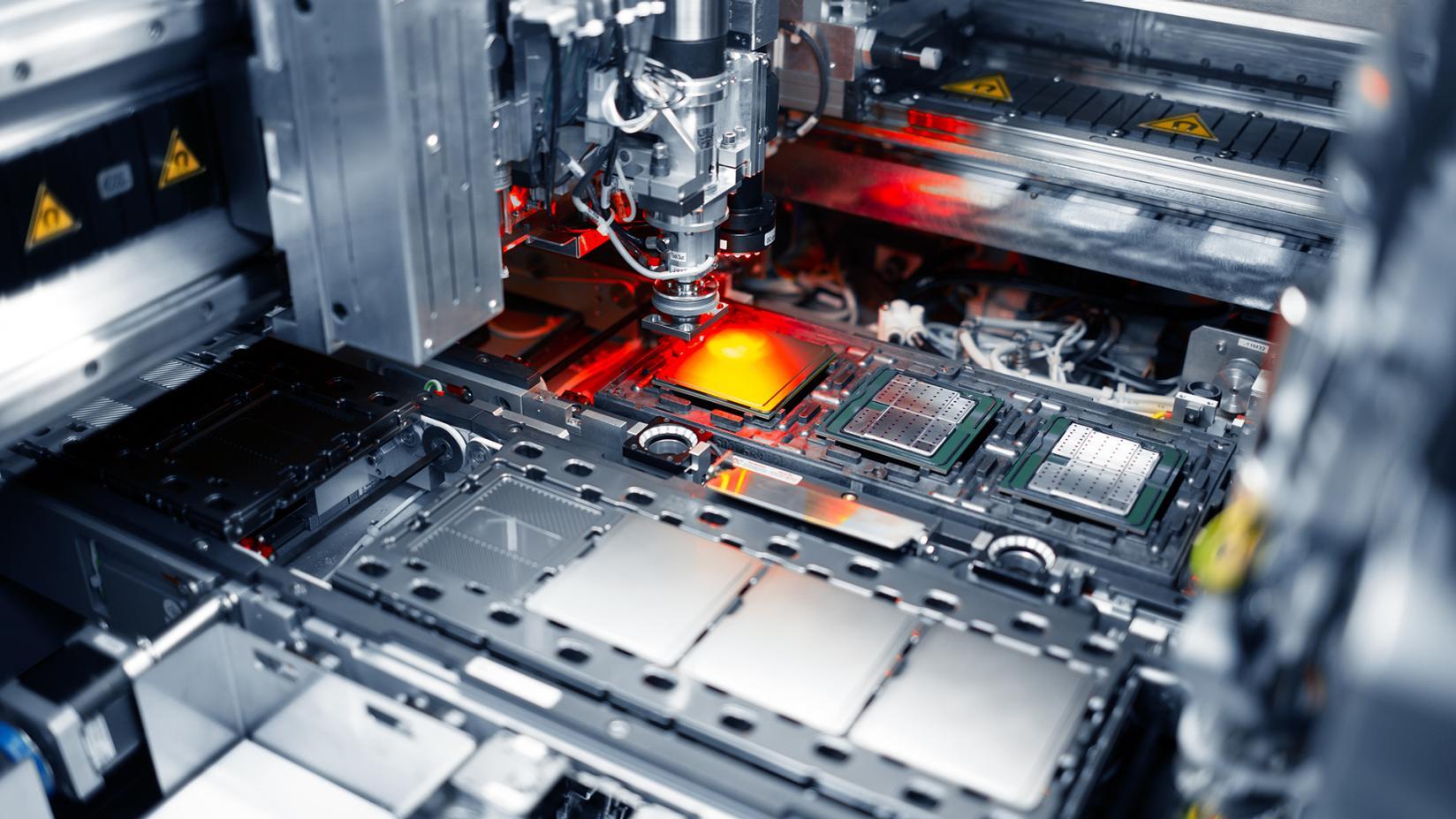
Intel is first to take delivery of its High-NA Extreme Ultraviolet Lithography machine
Intel CEO Gelsinger said, "I've bet the whole company on 18A." Intel expects that the performance and efficiency of its 18A node will top TSMC's best. Intel also inked a deal with Arm allowing Arm's chip-designing customers to have low-power SoCs built using Intel's 18A process node. Last month, Intel agreed to build a custom chip for Microsoft using its 18A process. Four unnamed large companies (it's not clear whether Microsoft is one of the four) have signed on to have Intel produce their chips using the 18A process.
Recently, Intel became the first company to take delivery of its $400 million High-NA Extreme Ultraviolet Lithography machine from Dutch manufacturer ASML. With billions of transistors stuffed inside application processors, the High-NA EUV can etch extremely thin circuitry patterns on silicon wafers.
The older EUV machines have an aperture of .33 (equivalent to a resolution of 13nm), and the High-NA machines have an aperture of .55 (equivalent to a resolution of 8nm). With a higher resolution pattern transferred to a wafer, the foundry could avoid having to run a wafer through the EUV machine twice to add additional features saving both time and money. While TSMC and Samsung Foundry have both ordered one of the High-NA machines from ASML, Intel will probably get to use the time-saving lithography machine first.

Readers’ Favorites

Latest News


Things that are NOT allowed:
To help keep our community safe and free from spam, we apply temporary limits to newly created accounts: