
Details about Samsung Foundry's 1.4nm process node surface

Why do we phone enthusiasts go nuts every time a foundry moves to a new process node? The most basic response I can think of is that as the process node drops, so does the size of the transistors used in a chip. Smaller transistors mean that more of them can fit inside a chip increasing the transistor count and the higher a transistor count, the more powerful and/or energy-efficient a chip is.
A good example that we use often is the iPhone. In 2019, the iPhone 11 line was powered by the 7nm A13 Bionic which contained 8.5 billion transistors. In 2020, the iPhone 12 line was equipped with the 5nm A14 Bionic which carried 11.8 billion transistors. That was followed the next year with the 5nm A15 Bionic used to power the iPhone 13 models. That chip carried 15 billion transistors. The iPhone 14 Pro series featured the 4nm A16 Bionic which contained 16 billion transistors. The iPhone 15 Pro and iPhone 15 Pro Max are currently the only smartphones using a 3nm chip, the A17 Pro, which has a transistor count of 19 billion.
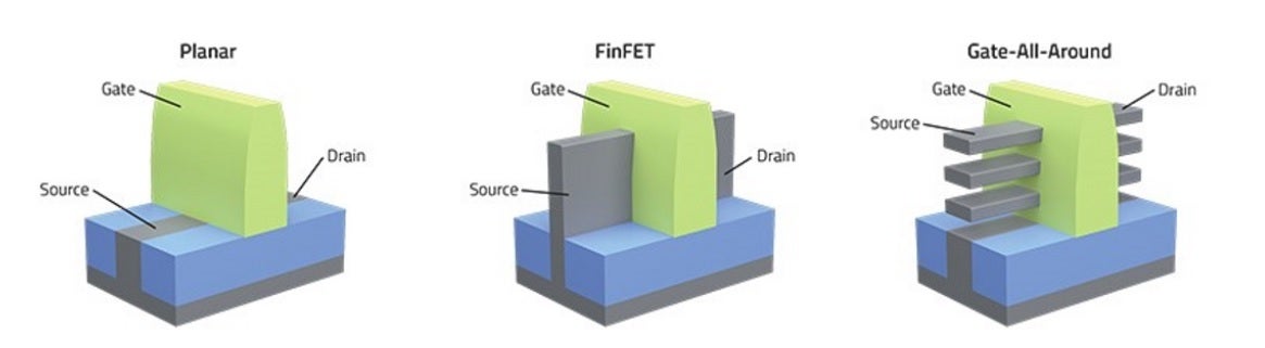
Right now, while both TSMC and Samsung Foundry can produce chips using their 3nm process nodes, there is a difference between the two firm's production at that node. While TSMC relies on FinFET transistors, Samsung Foundry uses the next-gen Gate-All-Around (GAA) transistors. Using three vertically placed horizontal nanosheets, GAA transistors surround the channel on all four sides of the gate. This reduces current leakage and boosts the drive current. TSMC will join Samsung and start using GAA with its 2nm process node.
By 2025, Intel, Samsung Foundry, and TSMC will all be using Gate-All-Around transistors
Samsung Foundry will also start mass-producing 2nm chips in 2025 and per Tom's Hardware, in 2027, it is expected to move to the 1.4nm process node. At 1.4nm, Samsung is expected to add a fourth nanosheet which will increase the drive current and improve the performance of a chip by allowing more current to flow through each transistor. Current leakage is reduced some more making chips produced at 1.4nm even more energy-efficient. With the increased control over current flow, the transistors manufactured at 1.4nm will generate less heat increasing power efficiency.
As we pointed out, Samsung is getting a head start over TSMC by using GAA now with its 3nm process node. And while TSMC won't join the club until it goes to 2nm in 2025, Intel will beat it out in 2024 with its 20A process node which will also use GAA (which it calls RibbonFET). By the time both Intel and TSMC start using GAA, Samsung will have experience with it.
All three foundries will also use backside power delivery at 2nm (20A for Intel which calls its version Power Via). This moves all power connections from the top of the chip to the bottom allowing more room for the data interconnects above the silicon and helps create larger power connections on the bottom of the chip. This will also lead to improved chip performance.

Popular stories


Latest News


Things that are NOT allowed:
To help keep our community safe and free from spam, we apply temporary limits to newly created accounts: