
The Canon machine that should have U.S lawmakers worried will start shipping this year or next year
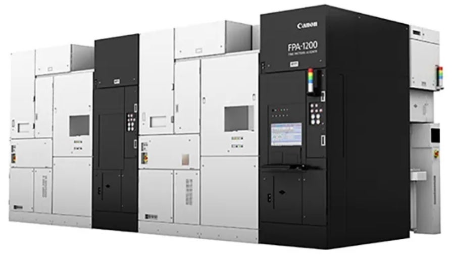
Last October we told you about Canon's nanoimprint lithography (NIL) technology that stamps the circuitry design onto a silicon wafer instead of etching it like ASML's extreme ultraviolet (EUV) machines do. The Financial Times (via Tom'sHardware) says that Canon has been working on this technology for 15 years and because it doesn't use lasers to create the pattern on a wafer, the process uses as much as 90% less power than a traditional EUV machine.
NIL technology can be used to build chips using a 5nm process node and eventually, it could be used to help produce 2nm chips. The lithography machine is important when it comes to chip manufacturing due to the billions of transistors that are found inside a chip. For example, the 3nm A17 Pro chipset inside the iPhone 15 Pro and iPhone 15 Pro Max carries 19 billion transistors. Circuitry patterns etched on wafers must be extremely thin.
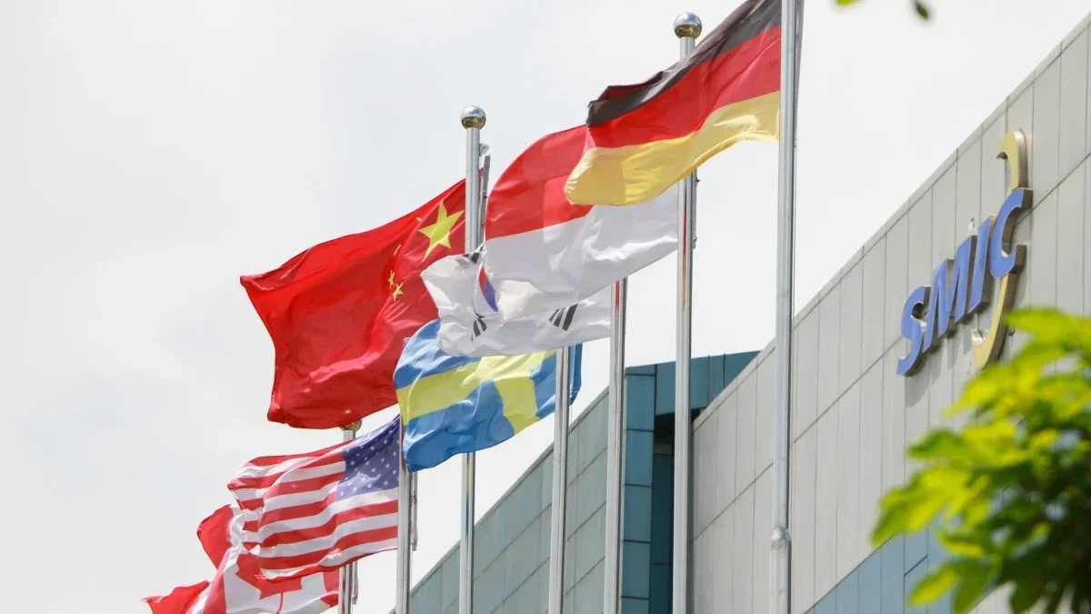
Here's why U.S. lawmakers could be sweating bullets over Canon's NIL machine. Currently, ASML, the only company in the world that makes EUV machines, is not allowed to ship these machines to China. It can and does deliver some of its deep ultraviolet machines (DUV) to the country. However, without the ability to obtain an EUV machine, China's largest foundry, SMIC, will not be able to build chips past the 7nm node it used to produce the 5G Kirin 9000s SoC used to power the Huawei Mate 60 series.
This is important because as the process node number drops, the transistors used on these chips become smaller allowing more of them to be shoehorned inside a chip. And the larger the number of transistors inside a chip, the more powerful and/or energy-efficient that chip is.
Cannon's NIL machine could help China's SMIC produce 5nm chipsets for Huawei
But if Canon isn't banned from shipping NIL machines to SMIC, all of a sudden the foundry might be able to produce 5nm chips bringing the country closer to the 3nm components that TSMC and Samsung Foundry are rolling off their assembly line this year. TSMC's 3nm node is already used to produce the A17 Pro application processor (AP) used with the iPhone 15 Pro line.
The worrying could be for nothing though, because it is not clear whether a fabrication process can be developed that solely relies on NIL technology. And NIL is not compatible with DUV or EUV so using NIL machines might not work with the current flow used by foundries to manufacture chips.
Speaking to The Financial Times, Richard Windsor, the head of research company Radio Free Mobile, said, "If nanoimprint technology was a superior technology, I think it would have been up and running by now and in the market in volume." While he might be right, there could be nothing that stops SMIC from trying to make NIL work so that it can build 5nm Kirin chips for Huawei. After all, Hiroaki Takeishi, chief of Canon's Optical Products Operations, told the Financial Times that NIL technology will allow for the creation of simple, low-cost, cutting-edge chips. That sounds exactly like what SMIC has in mind.
Current U.S. export rules prevent foundries using American technology from shipping cutting-edge chips to Huawei without obtaining a license and Takeishi says that he is eager for Canon to start shipping its NIL machines in 2024 and 2025.

Popular stories


Latest News


Things that are NOT allowed:
To help keep our community safe and free from spam, we apply temporary limits to newly created accounts: