China might be licking its lips as Canon reveals tech that could produce 2nm chips without EUV
There is but one company in the world that builds the $200 million school bus-sized EUV (extreme ultraviolet lithography) machines that are used to etch circuitry patterns thinner than human hair onto a silicon wafer. That company is ASML, a Dutch outfit that took in nearly $26 billion in revenue last year. EUV machines are necessary to manufacture chips under 7nm because you need to etch extremely fine lines to accommodate the billions of transistors that are packed into cutting-edge chips.
Canon announces a NIL lithography machine that could challenge EUV technology
Last week, Canon announced nanoimprint lithography (NIL) technology that it says can be used to produce 5nm chips. EUV machines are being used by TSMC and Samsung Foundry to manufacture 3nm chips with an upgraded machine from ASML coming soon to handle 2nm production. Both foundries expect to churn out 2nm chips as soon as 2025. But let's get back to Canon's announcement, shall we?
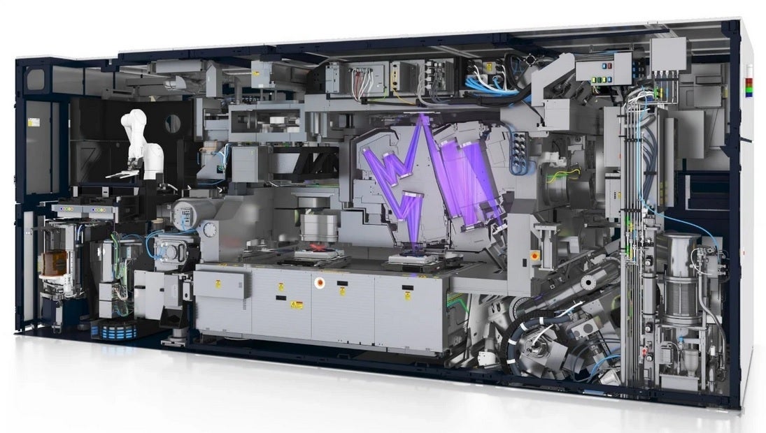
ASML's extreme ultraviolet lithography machine which is about the size of a school bus
The Japanese company explains what makes NIL different. "In contrast to conventional photolithography equipment, which transfers a circuit pattern by projecting it onto the resist coated wafer, the new product does it by pressing a mask imprinted with the circuit pattern on the resist on the wafer like a stamp. Because its circuit pattern transfer process does not go through an optical mechanism, fine circuit patterns on the mask can be faithfully reproduced on the wafer. Thus, complex two- or three-dimensional circuit patterns can be formed in a single imprint."
Canon says that with improvements to mask technology, NIL will eventually be able to help create 2nm chips. Currently, the technology can etch circuit patterns with a minimum linewidth of 14 nm which equates to 5nm production. Canon says that NIL is expected to support a minimum linewidth of 10 nm which equates to building chips using a 2nm process node. NIL can reduce the amount of power used to manufacture a chip since it doesn't require a lightsource with a special wavelength.
Despite the press release, Gartner analyst Gaurav Gupta told The Register, "I would be surprised if there is a major technical breakthrough that Canon has suddenly achieved." Nanoimprint lithography has been a concept for some time, but there have been issues with defects and other problems. Memory chip developer SK Hynix and electronics firm Toshiba signed a pact back in 2015 to develop NIL.
But there is a problem here that the U.S. will have to address quickly. ASML does not ship its EUV machines to China due to U.S. sanctions, but it is possible that since NIL doesn't use cutting-edge optics or mirrors like EUV does, Canon might be able to ship the technology to China giving foundries like SMIC (the largest in China) the ability to produce 5nm and eventually 3nm and 2nm chips.
We've seen how U.S. lawmakers and officials reacted when Huawei unveiled the Mate 60 Pro powered by a 7nm Kirin 9000s chip that supports 5G. To this day, there are elaborate theories that try to explain how SMIC was able to manufacture the chip considering the current U.S. export ban. One theory that an X tipster posted last week was that the Kirin 9000s was not a 7nm chip made by SMIC, but was actually an older Kirin 9000 SoC from Huawei's inventory. The latter was made by TSMC before the ban started in 2020 using its 5nm process node.
Gartner's Gupta says, "We don't expect commercial impact before five years and to start primarily with memory chips. There is a big gap in research and development or concept capability at leading-edge nodes… vs. high-volume execution and [being] manufacturing ready, and that's the challenge." He expects that the U.S. will move to block the sale of this technology to China soon.

Popular stories


Latest News


Things that are NOT allowed:
To help keep our community safe and free from spam, we apply temporary limits to newly created accounts: