How TSMC and ASML plan to get to the 2nm process node

With the release tomorrow of the Apple iPhone 12, iPhone 12 Pro, and the iPad Air (2020), consumers around the globe will get to experience a 5nm chipset for the first time. Built by TSMC, the number one independent foundry on the planet, Apple's A14 Bionic shoehorns an unimaginable 11.8 billion transistors inside an integrated circuit. That compares to the 8.5 billion transistors employed by the A13 Bionic.
TSMC, ASML look ahead to 3nm and 2nm chips
Huawei's 5nm Kirin 9000 powers the Mate 40 series, but unlike Apple, the number of 5nm Kirin chips is limited because of a U.S. Commerce Department rule change that prevents foundries using American made tech from shipping to Huawei. The company ordered 15 million 5nm chips but only received 8.8 million until the rule change kicked in during the middle of September. Huawei not only uses its 5nm chip to power its new flagship phone but also uses it to power 5G network base stations and the sequel to its foldable phone (the Mate X2). Next year Samsung will reportedly release two 5nm Exynos chips while Qualcomm will join the club with the Snapdragon 875.
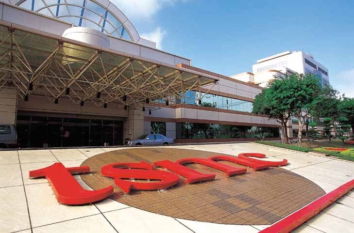
TSMC is working on 3nm and 2nm process nodes
But companies like TSMC and Samsung won't even have time to pat themselves on the back over their 5nm components. That's because both foundries are already working on the 3nm process node. Back in 1965, Intel co-founder Gordon Moore observed that the transistor density on a chip doubled every year. He later revised that to a doubling of transistor density every other year. So that leaves little time to celebrate.
One of the tools developed to keep Moore's Law alive is extreme ultraviolet (EUV) lithography. Lithography is used to print circuits on thin slices of silicon. When you think about the size of a chipset and the billions of transistors that need to be placed inside it, you can understand that extremely thin markings need to be made inside a chip. EUV uses ultraviolet beams to make this possible. The N5 node that TSMC is working with can use 5nm for up to 14 layers. The 3nm process node could deliver up to a 15% hike in power at the same transistor count as 5nm, and up to a 30% reduction in power use (at the same clock speeds and complexity).
Dutch lithography company ASML says that at 3nm, lithography can be used on more than 20 layers. Peter Wennink, CEO of ASML, says that "I think, on the N5 in logic we are over 10 layers and in N3 we will be over 20 and we actually see that creeping up. That has just the fact that it gives so much more advantage to go to single patterning and take away these multi patterning DUV (Deep ultraviolet) strategies, which is also true for DRAM." When a single lithography exposure does not produce a sharp resolution print, double patterning exposures are used. Memory (RAM and NAND) chip manufacturers rely on this process.
TSMC plans on using FinFET transistors for its 3nm mode before switching to GAAFET (gate all around) for 2nm chips. Unlike FinFET, which doesn't surround a channel on all sides, GAA surrounds a channel using a Gate. The latter method makes current leakage almost negligible.
Peter Wennink, Chief Executive Officer of ASML, says that the company must follow the U.S. Commerce Department rules when it comes to shipping lithography systems to Chinese foundries like SMIC. The executive said, "ASML requires a U.S. export license for systems or parts that are shipped directly from the U.S. to customers affected by the rules. While it is not a policy to comment on individual customers, we aim to serve and support all of our customers around the world to the best of our abilities, whilst being, of course, compliance with laws and regulations set by the jurisdictions where we operate. SMIC is the largest foundry in China and currently it is working on a 7nm process node while its most cutting edge production is done at 14nm. SMIC needs more advanced lithography machines but is currently stymied by the U.S. Commerce Department rule change.










Things that are NOT allowed:
To help keep our community safe and free from spam, we apply temporary limits to newly created accounts: