World's first 2nm chip is produced by IBM
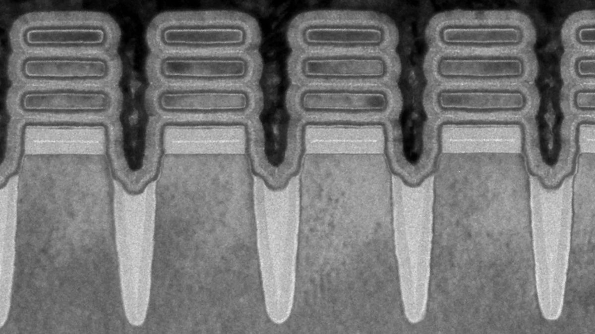
When it comes to the companies whose components power smartphones, IBM is not a name that comes to mind. Today, though, Big Blue announced that it has created a transistor for the 2nm process node using Gate-All-Around (GAA) nanosheet device architecture that will allow IBM "to fit 50 billion transistors in a space roughly the size of a fingernail."
Current cutting-edge chips like the Apple A14 Bionic and the Snapdragon 888 are using the 5nm process node. Using the former as an example, the A14 Bionic fits 134.09 million transistors into a square mm, up from the 89.97 million on the A13 Bionic. The total number of transistors packed inside the A14 is 11.8 billion compared to 8.5 billion used on the A13 Bionic.
IBM unveils the world's first 2nm chip
The larger the number of transistors that fit in a square mm space, the more powerful and energy-efficient that chip is. From the 7nm process node used on the A11 Bionic and Snapdragon 865 to the 2nm node that IBM is writing about, the performance increase amounts to 45% using the same amount of power. That works out to a 75% power savings at the same power level.
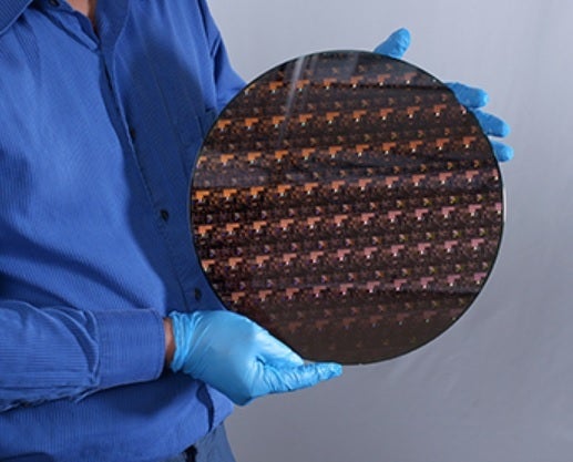
Chips are cut out of wafers like the 11.8-inch wafer used for 5nm chips
To help cram billions of transistors inside a chip, IBM uses Extreme Ultraviolet Lithography (EUV), which produces lines smaller than visible light. These lines create the patterns that will be used to create circuits. IBM also replaced the FinFET architecture with GAA and as IBM puts it, "Four “gates” on a transistor enable superior electrical signals to pass through and between other transistors on a chip."
IBM says that using a 2nm chip could do wonders for battery life on smartphones. The company says, "Put in perspective, 2nm processors used in cell phones could quadruple the battery life of cell phones using 7nm process technology, such as the iPhone 11, Samsung Galaxy S10 and Google Pixel 5. Based on average use, this means the phone would only need to be charged once every four days."
And for those worried that we're coming to the end of Moore's Law (the observation made by Intel co-founder Gordon Moore that the transistor density in chips doubles every other year), IBM Research says that it "continues to explore options for continued scaling to 1nm and beyond."
IBM says that it is still several years from manufacturing its 2nm node devices and that this year it will debut its first commercialized 7nm processor. Next year, TSMC and Samsung Foundry are expected to begin volume production of chips using the 3nm process node.
The fact that IBM has made the world's first 2nm chip is a big boost to the U.S. chip industry. Last year, the world's top foundry, TSMC, announced that it was building a $12 billion fab in Arizona and a new report says that the U.S. has requested that five additional fabs be built for a total of six. The U.S. is trying to take chip production out of Asia so that global manufacturers don't have to be concerned about the relationship between China and other countries.
There is concern that China, if it gets desperate enough for chips, will attack Taiwan in a bid to take control of TSMC which counts Apple as its biggest customer. IBM is headquartered in the U.S. and the 300mm wafer (11.81-inches) used for the 2nm chips was produced at IBM Research's semiconductor research facility in Albany, NY.
The company stated that "our demonstration of a nanosheet transistor for the 2 nm chip node is also a validation of several smaller milestones that proved to us this could be done, and of the hard work and dedication of IBM’s interdisciplinary team of experts in materials, lithography, integration, devices, characterization and modeling working on the project."

Popular stories


Latest News


Things that are NOT allowed:
To help keep our community safe and free from spam, we apply temporary limits to newly created accounts: