We’re slowly moving toward the size limitations of our Universe but before we reach that Planck volume, there’s still some wiggle room. This means smaller, faster, and more efficient chips in our smartphones of tomorrow.
Let’s leave quantum physics behind, and go straight to the news (feel free to discuss Planck constants in the comment section below). After TSMC published its roadmap, shedding light on when we can expect 3nm and 2nm chips, now Samsung has announced the production start of its 3nm semiconductor chips in Hwaseong factory in South Korea.
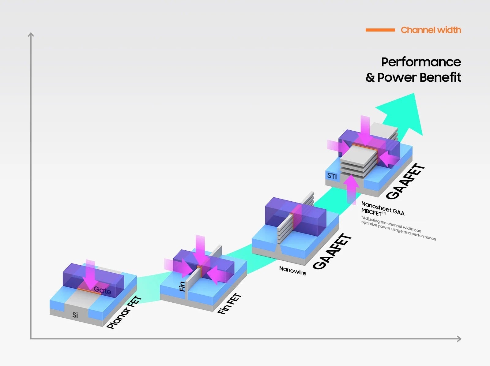
Samsung is moving to a new architecture, swapping FinFET (fin field-effect transistor) for GAA (Gate All Around). And if you’re worried that more physics is coming your way, just breathe. GAA offers several advantages over FinFET - the main one being higher power efficiency.
Another new technology involved in Samsung’s 3nm manufacturing node is the nanosheet transistor manufacturing. It replaces the nanowire technology, again boosting efficiency and also performance in this case. Using nanosheets gives the ability to very easily adjust this efficiency and performance parameters by simply altering the size of the nanosheet.
Samsung is quoting some impressive numbers, comparing the new 3nm node with the old 5nm manufacturing process. The new chips should come with 23% improved performance, a 45% reduction in power usage, and an area reduction of 16%, and this is just the first generation of 3nm silicon.
Samsung is moving from FinFET and nanowire technology to GAA and nanosheets
The second generation will bring a hefty 50% increase in power efficiency, 30% better performance, and 35% less area. Here’s a little inspirational quote from Dr. Siyoung Choi, President and Head of Foundry Business at Samsung Electronics:
Recommended For You
“Samsung has grown rapidly as we continue to demonstrate leadership in applying next-generation technologies to manufacturing, such as foundry industry’s first High-K Metal Gate, FinFET, as well as EUV. We seek to continue this leadership with the world’s first 3nm process with the MBCFETTM. We will continue active innovation in competitive technology development and build processes that help expedite achieving maturity of technology.”
The Korean company is also working to allow clients to design their chips faster and easier. Samsung's SAFE ((Samsung Advanced Foundry Ecosystem) will be taking care of partners who want to design their 3nm chips using the new technology.
The first 3nm smartphone processor leaving the factory will most likely be the next generation Exynos 2300 (S5E9935 codename Quadra). The jump to GAA and 3nm could rehabilitate the Exynos processors, which are not very popular among smartphone enthusiasts, and are lagging behind their Qualcomm counterparts. Samsung teamed up with AMD to try and turn things around (the Exynos 2200 is armed with the new Xclipse GPU based on AMD RDNA 2 architecture) but this partnership has yielded mixed results so far.
With TSMC hiking the prices of its manufacturing processes, it's also very interesting to see how would Samsung play its cards on that front. If the new 3nm node turns out to be cheaper at Samsung's factories, it can swing the pendulum once again. On the other hand, don't expect the next Galaxy S23 with Exynos onboard to be cheaper than the Qualcomm variant, as it won't make any marketing sense.
Mint Mobile is now allowing you to get whichever plan you like for either three, six, or 12 months for just $15/mo. If you go for the six-month unlimited service, for instance, you'll now have to pay just $90 upfront instead of $210.
Mariyan, a tech enthusiast with a background in Nuclear Physics and Journalism, brings a unique perspective to PhoneArena. His childhood curiosity for gadgets evolved into a professional passion for technology, leading him to the role of Editor-in-Chief at PCWorld Bulgaria before joining PhoneArena. Mariyan's interests range from mainstream Android and iPhone debates to fringe technologies like graphene batteries and nanotechnology. Off-duty, he enjoys playing his electric guitar, practicing Japanese, and revisiting his love for video games and Haruki Murakami's works.
A discussion is a place, where people can voice their opinion, no matter if it
is positive, neutral or negative. However, when posting, one must stay true to the topic, and not just share some
random thoughts, which are not directly related to the matter.
Things that are NOT allowed:
Off-topic talk - you must stick to the subject of discussion
Offensive, hate speech - if you want to say something, say it politely
Spam/Advertisements - these posts are deleted
Multiple accounts - one person can have only one account
Impersonations and offensive nicknames - these accounts get banned
To help keep our community safe and free from spam, we apply temporary limits to newly created accounts:
New accounts created within the last 24 hours may experience restrictions on how frequently they can
post or comment.
These limits are in place as a precaution and will automatically lift.
Moderation is done by humans. We try to be as objective as possible and moderate with zero bias. If you think a
post should be moderated - please, report it.
Have a question about the rules or why you have been moderated/limited/banned? Please,
contact us.


Things that are NOT allowed:
To help keep our community safe and free from spam, we apply temporary limits to newly created accounts: