After Apple unveils two powerful 5nm chips, TSMC introduces its latest N4P process node

The world's leading contract foundry, TSMC, announced today its N4P process which is an enhancement of the 5nm platform. Considered the third enhancement of TSMC's 5nm line, N4P will deliver an 11% performance hike over the original generation N5 technology and a 6% hike over N4. Power efficiency of the N4P process is 22% better than with the OG N5 process and transistor density (the number of transistors that fit in a square mm) is 6% higher.
TSMC says that "N4P joins the industry's most advanced and extensive portfolio of leading-edge technology processes. With N5, N4, N3, and the latest addition of N4P, TSMC customers will have multiple and compelling choices for power, performance, area, and cost for its products. With the addition of N4P, can give its customers "multiple and compelling choices for power, performance, area, and cost for its products."
TSMC introduces its new N4P process node
The amount of time it takes to process a wafer lot (usually 25 wafers) is improved by reducing the number of masks needed to transfer circuity patterns onto the wafers. The foundry says, "N4P demonstrates TSMC's pursuit and investment in continuous improvement of our process technologies." The company adds, "The N4P process was designed for an easy migration of 5nm platform-based products, which enables customers to not only better maximize their investment but will also deliver faster and more power efficient refreshes to their N5 products."

TSMC announces its new N4P process node
Dr. Kevin Zhang, Senior Vice President of Business Development at TSMC, added that "With N4P, TSMC strengthens our portfolio of advanced logic semiconductor technologies, each with its unique blend of performance, power efficiency and cost. N4P was optimized to provide a further enhanced advanced technology platform for both HPC and mobile applications." The first tape-outs of N4P will appear by the second half of next year.
The executive adds that "Between all the variants of N5, N4 and N3 technologies, our customers will have the ultimate flexibility and unmatched choice of the best mix of attributes for their products." There was no comment made about the global chip shortage that has started to impact the production of the Apple iPhone and iPad. The Cupertino-based firm is the foundry's biggest customer.
TSMC also didn't mention the delay it announced in August with its 3nm process node. This will force the foundry to produce next year's A16 Bionic chipset using the 4nm process node instead of the 3nm process originally expected. This year's iPhone 13 line is powered by the A15 Bionic, a chipset manufactured using TSMC's enhanced 5nm process (N5P) that features 15 billion transistors up from the 11.8 billion employed on the A14 Bionic SoC used on the iPhone 12 series.
This is the first time since 2014 that TSMC has had to announce a delay in introducing a process node for Apple's A-series chipsets. Back then, TSMC was having issues building the 20nm chip that Apple was going to use to power the iPhone 6 and iPhone 6 Plus.
Apple introduces two new powerful M-series chips
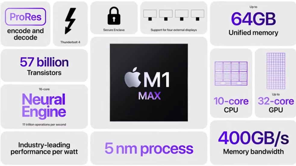
Despite the chip shortage, Apple just recently announced two new powerful chipsets for its M-series high-performance line. The M1 Pro and M1 Max will sport 33.7 billion and 57 billion transistors respectively and will be built using the 5nm process node. Compare the transistor count on those two new chips with the 16 billion used with the M1.
The M-series chips are designed by Apple to replace the Intel processors it formerly used on Macs. Apple did endow the 11-inch and 12.9-inch iPad Pro (2021) tablets with the M1.
TSMC's top competitor, Samsung Foundry, also is delaying the release of its 3nm chipsets. Leakage issues have reportedly forced Samsung to delay the volume production of its 3nm GAA (Gate All Around) chips. The Qualcomm Snapdragon 898, the next flagship chip in the Snapdragon family, will reportedly roll off of Sammy's assembly lines using the 4nm process node.
Earlier reports hinted at a 20% performance boost for the chip, which is expected to be found under the hood of Samsung's next Galaxy S22 flagship when those handsets are released, most likely early next year. Both TSMC and Samsung have produced roadmaps taking production down to the 2nm process node, although both are dealing with the unexpected detour at 3nm.


Things that are NOT allowed:
To help keep our community safe and free from spam, we apply temporary limits to newly created accounts: