China's SMIC may have used older lithography gear to build Huawei's new 5nm chip
Huawei might have worried U.S. lawmakers by producing 5nm chips using older lithography equipment.

China's largest foundry, SMIC, is also the third-largest foundry in the world. Thanks to U.S. and Dutch sanctions, the foundry cannot obtain cutting-edge lithography machines. Without the ability to use extreme ultraviolet lithography machines (EUV) to transfer circuitry patterns to silicon wafers, SMIC was believed to be limited to producing chips using its 7nm node. We are now in the middle of an interesting mystery.
Huawei's new Mate Book Pro laptop runs HarmonyOS and is powered by the Kirin X90 chip designed by Huawei's HiSilicon chip design unit. One leaker says that the X90 is a repurposed Kirin 9010 with a different layout of the CPU cores. We should know for sure sometime over the next few days when in-depth reviews of the chip are expected to be released. The Kirin 9010 AP was used to power Huawei's photography-based Pura 70 flagship series that was released in April 2024 and it was built using SMIC's 7nm N+2 process node.
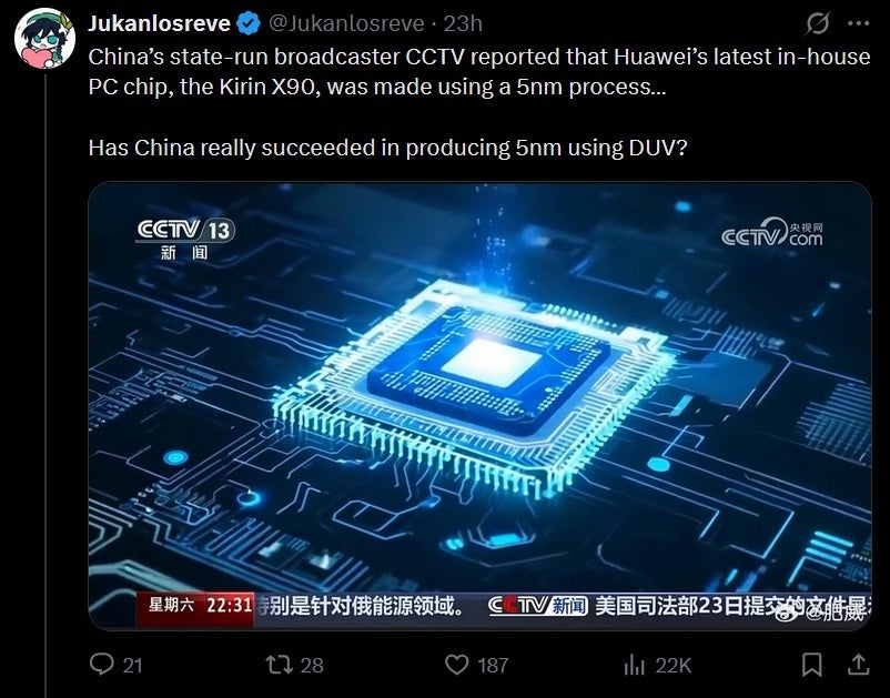
However, a Chinese news channel has reported some shocking information. According to this station's report, the X90 is actually manufactured using SMIC's 5 nm N+3 node. Last year we passed along several rumors about SMIC's ability to produce 5nm chips without using EUV. One report said that SMIC used older Deep Ultraviolet (DUV) lithography machines, purchased before any sanctions were imposed, to manufacture 5nm chips. Multiple impressions onto silicon wafers were made allowing the circuitry patterns to work through the blurriness created by using DUV's 193nm wavelengths for 5nm features.

Did SMIC really build a 5nm chip using DUV? | Image credit-X
A tweet on "X" from leaker @Jukanlosreve credited Chinese state-run broadcaster CCTV with running the report about the 5nm node for the X90. Another X user, @zephyr_z9, claims that the Kirin X90 has a transistor density of 125 million transistors per mm2. That makes it less dense than TSMC's 5nm node (approximately 138 million transistors per mm2) but close to the density used with Samsung Foundry's 5nm node. What makes this amazing is that it appears to have been achieved using a DUV machine.
Not all of the numbers were positive. One analyst reportedly discovered that SMIC is producing 3,000 wafers per month with an extremely low 20% yield. Most foundries want to see a minimum yield of 70% before starting mass production of a chip.
Despite the anemic yield, if SMIC is able to produce 5nm chips using DUV, this will worry U.S. lawmakers who have been concerned about Huawei's ability to design cutting-edge silicon for the Chinese military and AI even with U.S. sanctions.


Things that are NOT allowed:
To help keep our community safe and free from spam, we apply temporary limits to newly created accounts: