
Huawei files patent for low-tech lithography method that might help it build a 5nm SoC
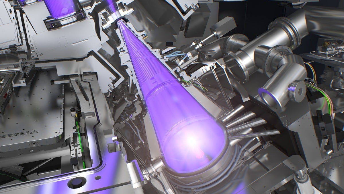
According to SemiWiki, late last month it was discovered that Huawei and a chip-making partner backed by the Chinese government are working on a low-tech way to replace the extreme ultraviolet lithography machines that Chinese companies can't obtain because of U.S. and Dutch restrictions. These machines etch extremely thin circuitry patterns on silicon wafers and help foundries place billions of transistors inside chipsets. The EUV machines are made by one manufacturer, Dutch firm ASML.
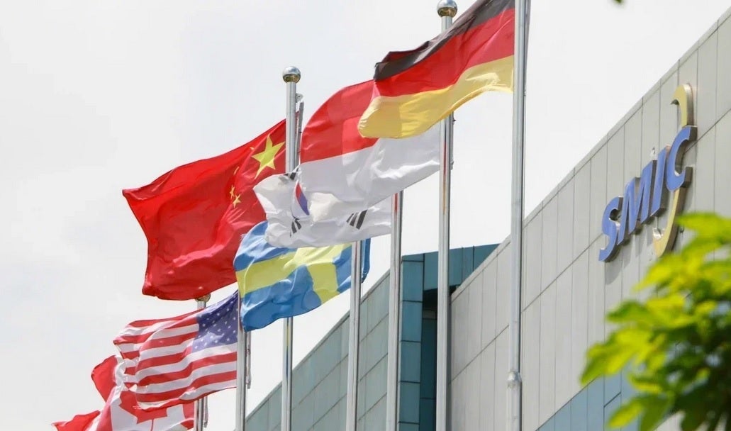
The 7nm Kirin 9000s 5G application processor (AP) built by China's SMIC, the largest foundry in the country, was used by Huawei for the Mate 60 series it shocked the world with last August. It was the first 5G chip used on a Huawei phone since 2020's Mate 40 Pro and SMIC is believed to have built the components using the deep ultraviolet lithography machines that it has been allowed to buy from ASML over the years. The problem for SMIC is that DUV machines can't be used to produce 5nm chipsets and Huawei needs to obtain more advanced chips if it is going to continue to overcome the U.S. sanctions that have negatively impacted Huawei over the last four years.
SMIC built the Mate 60 series' Kirin 9000s 5G AP using its 7nm node
Huawei and its partner have filed patents for a process called "self-aligned quadruple patterning," or SAQP, and this could allow Huawei or SMIC to build advanced chips. Quadruple patterning etches the circuitry patterns into the silicon wafer multiple times which can increase transistor density and the performance of the AP.
Huawei's patent application, filed with the China National Intellectual Property Administration, was released on Friday and the filing said, "Adoption of this patent will increase the design freedom of circuit patterns." The state-backed company working with Huawei to develop the new lithography technology is called SiCarrier and it received a patent last year for a technique that uses SAQP and deep ultraviolet lithography to produce chips that have the characteristics of components made using the 5nm process node.
The patent said that the technique can help SMIC and Huawei avoid having to get access to a EUV machine (which, as noted above, it is blocked from doing now by U.S. and Dutch sanctions) and reduce manufacturing costs. Dan Hutcheson, vice-chairman at research firm TechInsights, says that quadruple-patterning should help China make 5nm chips but in the long run it still needs to get its hands on an EUV machine.
With China currently building smartphone chipsets at 7nm, the country remains two generations behind the 3nm node that TSMC used to build the A17 Pro AP currently powering the iPhone 15 Pro and iPhone 15 Pro Max. This gap explains why the Chinese are so desperate to somehow bypass EUV lithography.

Popular stories


Latest News


Things that are NOT allowed:
To help keep our community safe and free from spam, we apply temporary limits to newly created accounts: