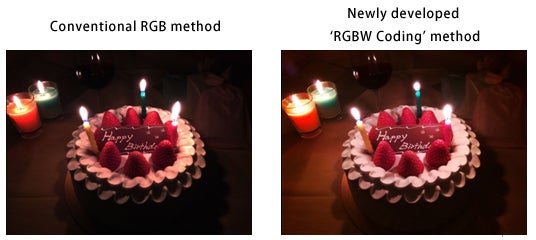
Moreover, these sensors allow you to shoot HDR video on the fly, and the first one found its place in the 13MP Sony Xperia GX, which is bound to hit Japan next month.
Apple, Samsung and, of course, Sony, are using the company's sensors in their smartphones, so it will be interesting to see whether the "stacked" tech will make its way into the new iPhone 5 that is bound to arrive in the fall.
It might not be accidental that the Japanese are investing $994 million to expand plant production to 60, 000 wafers a month for making many of those stacked camera sensors.
Sony increases production capacity for stacked CMOS image sensors
- Increasing total production capacity for image sensors to approximately 60,000 wafers per month to supply image sensors mainly for smartphones -
June 22, 2012, Tokyo, Japan – Sony Corporation ("Sony") today announced that it plans to invest in Sony Semiconductor Corporation's Nagasaki Technology Center ("Nagasaki TEC") from the first half of the fiscal year ending March 31, 2013 through the first half of the fiscal year ending March 31, 2014, to increase the production capacity for stacked CMOS image sensors.*1
This investment is intended to provide for new wafer processing equipment for stacked CMOS image sensors, and to increase and transform wafer lines capable of manufacturing CMOS image sensors.
With this development, Sony plans to increase total production capacity for CCD and CMOS image sensors to approximately 60,000 wafers per month by the end of September 2013.*2
In light of the rapidly expanding demand for smartphones and tablets, Sony plans to continue to solidify its leading global position in CMOS image sensors by strengthening its production capabilities for stacked CMOS image sensors, which provide greater performance in a more compact form. Furthermore, Sony intends to accelerate its growth strategy by incorporating superior core technologies, including stacked CMOS image sensors, into a wide range of products for its digital imaging and mobile businesses, which are priorities within its electronics business.
The investment amount is approximately 80 billion yen, of which, the amount to be invested in the current fiscal year ending March 31, 2013 (approximately 45 billion yen) was included in the forecast of the capital expenditures for semiconductors in the current fiscal year announced at the annual earnings release on May 10, 2012. In addition, Sony will utilize a governmental subsidy in its investment plan which will be provided by the Ministry of Economy, Trade and Industry in Japan, through the "Subsidy for Domestic Location Promotion Projects" program.
Get Visible as low as $20/mo for 1 year. Limited time offer with code: FRESHSTART
$20
/mo
$25
$5 off (20%)
Offer Ends 6.1.2026 at 11.59pm ET. New members get $5/mo off the $25/mg Visible plan, $35/mo Visible+ plan, or $45/mo Visible+ Pro plan for the first 12 months. Promo code FRESHSTART required at checkout.
Daniel, a devoted tech writer at PhoneArena from 2010 to 2025, has been engrossed in mobile technology since the Windows Mobile era. His expertise spans mobile hardware, software, and carrier networks, and he's keenly interested in the future of digital health, car connectivity, and 5G. Beyond his professional pursuits, Daniel finds balance in travel, reading, and exploring new tech innovations, while contemplating the ethical and privacy implications of our digital future.
Recommended For You
COMMENTS (23)
COMMENTS (23)
All comments need to comply with our
Community Guidelines
PhoneArena Community Rules
A discussion is a place, where people can voice their opinion, no matter if it
is positive, neutral or negative. However, when posting, one must stay true to the topic, and not just share some
random thoughts, which are not directly related to the matter.
Things that are NOT allowed:
Off-topic talk - you must stick to the subject of discussion
Offensive, hate speech - if you want to say something, say it politely
Spam/Advertisements - these posts are deleted
Multiple accounts - one person can have only one account
Impersonations and offensive nicknames - these accounts get banned
To help keep our community safe and free from spam, we apply temporary limits to newly created accounts:
New accounts created within the last 24 hours may experience restrictions on how frequently they can
post or comment.
These limits are in place as a precaution and will automatically lift.
Moderation is done by humans. We try to be as objective as possible and moderate with zero bias. If you think a
post should be moderated - please, report it.
Have a question about the rules or why you have been moderated/limited/banned? Please,
contact us.


Things that are NOT allowed:
To help keep our community safe and free from spam, we apply temporary limits to newly created accounts: