Batteries. Those little buggers are the reason we’re still struggling with electric vehicles and charging our smartphones almost every day. The good old lithium battery is decades old now, and even though there are numerous advancements such as solid-state batteries, graphene-cathode batteries, supercapacitors, etc., the reality is that these prototypes are still years away from mass production and from our electronic gadgets.
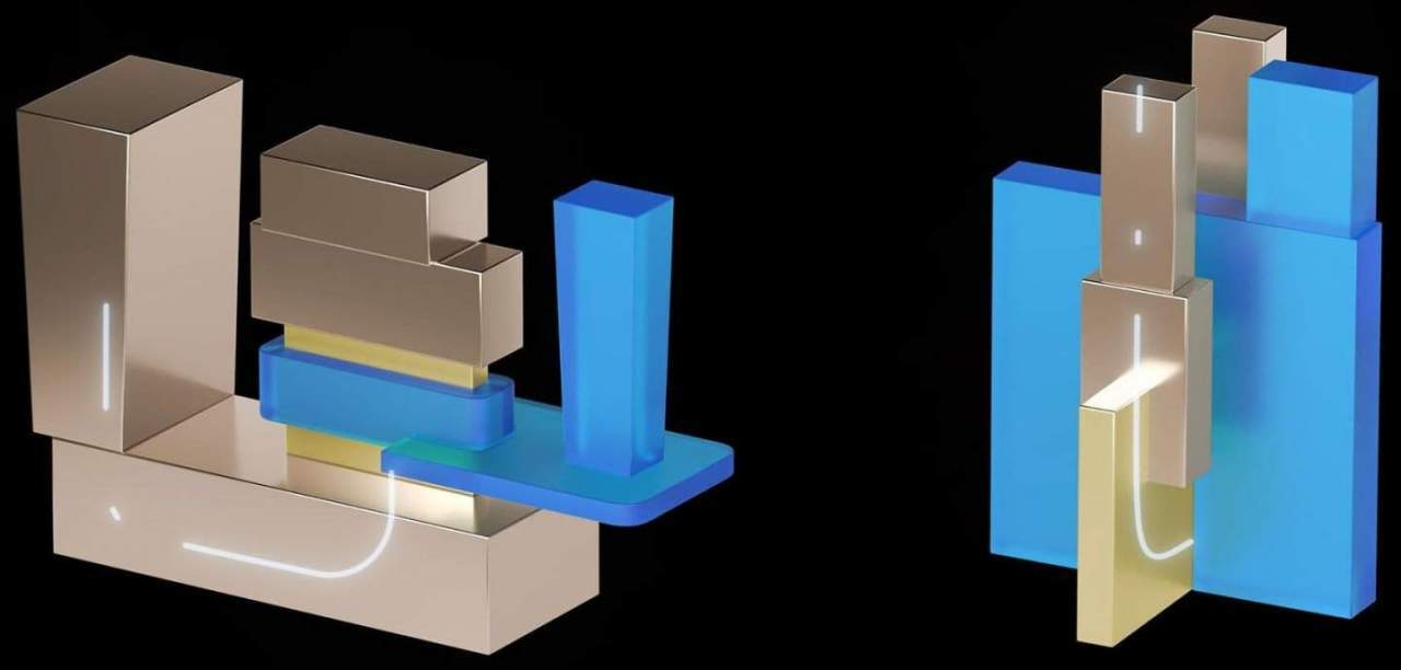
Now Samsung and IBM have employed a completely different approach. Instead of trying to increase battery capacity, the tech giants are developing a new kind of chip architecture that can potentially cut energy consumption by up to 85%. This new technology can effectively help smartphones last weeks on a single charge, and it’s called Vertical-Transport Nanosheet Field Effect Transistor (VTFET).
Most modern chips (like the Snapdragon inside your Android phone, or the A15 bionic inside your iPhone) are based on lateral-transport field-effect transistors (finFET). Without delving deep into electronics, this means that the transistors inside the chips are arraigned on a wafer-like flat surface - the signal travels back and forth in a 2D manner (so to speak).
The new VTFET design just takes this design and expands it in a vertical direction (much like the VNAND flash that Samsung is making). By laying transistors on top of each other, IBM and Samsung were able to bypass certain limitations in the conventional design - offer better contact size and surface, and optimize transistors’ gate length.
Recommended For You
As a result, the new design can be optimized in two different ways - either by going for efficiency - where the performance would be more or less on par with modern ARM architectures like the aforementioned Snapdragon and Bionic chipsets. However, due to the increased efficiency, this approach would yield up to an 85% increase in battery life - practically solving the charging conundrum in modern smartphone technology.
The other approach would be to increase the performance of the chip, matching the energy consumption of the modern flat designs. Going this route would grant a 100% increase in performance, compared to modern FET alternatives.
Of course, we’re talking about early lab prototypes but tech experts from IBM say that this new design has the potential for “scaling beyond nanosheet.” What this means is that going from a simple prototype to mass-produced consumer chips shouldn’t be that hard.
VTFET transistor architecture - IBM
The potential applications of this new transistor design are endless - who doesn’t need efficiency and increased performance? Apart from allowing smartphone batteries to last for up to a whole week, the VTFET design could cut the energy used to mine crypto, and given the hype around blockchain technology, this could be huge.
Another field that would massively benefit the new designs is IoT - allowing for even tinier devices that could run for months. IBM and Samsung also emphasize that this new breakthrough could also extend Moore’s law (stating that transistor count doubles every couple of years), which has been put on hold (or at least slowed down significantly) in modern chips.
Again, this idea is very similar to vertical NAND flash memory modules, where memory cells are stacked on top of each other (thus allowing for greater size and cheaper price per GB of storage). The new VTFET design also aligns with IBM’s effort to reduce the footprint of transistors and chips in general - the company showcased its 2nm node technology back in May. This 2nm manufacturing process allows to pack up to 50 billion transistors on a chip the size of a fingernail.
We’re still a long way from seeing this design in consumer electronics but the future looks bright.
Mariyan, a tech enthusiast with a background in Nuclear Physics and Journalism, brings a unique perspective to PhoneArena. His childhood curiosity for gadgets evolved into a professional passion for technology, leading him to the role of Editor-in-Chief at PCWorld Bulgaria before joining PhoneArena. Mariyan's interests range from mainstream Android and iPhone debates to fringe technologies like graphene batteries and nanotechnology. Off-duty, he enjoys playing his electric guitar, practicing Japanese, and revisiting his love for video games and Haruki Murakami's works.
A discussion is a place, where people can voice their opinion, no matter if it
is positive, neutral or negative. However, when posting, one must stay true to the topic, and not just share some
random thoughts, which are not directly related to the matter.
Things that are NOT allowed:
Off-topic talk - you must stick to the subject of discussion
Offensive, hate speech - if you want to say something, say it politely
Spam/Advertisements - these posts are deleted
Multiple accounts - one person can have only one account
Impersonations and offensive nicknames - these accounts get banned
To help keep our community safe and free from spam, we apply temporary limits to newly created accounts:
New accounts created within the last 24 hours may experience restrictions on how frequently they can
post or comment.
These limits are in place as a precaution and will automatically lift.
Moderation is done by humans. We try to be as objective as possible and moderate with zero bias. If you think a
post should be moderated - please, report it.
Have a question about the rules or why you have been moderated/limited/banned? Please,
contact us.


Things that are NOT allowed:
To help keep our community safe and free from spam, we apply temporary limits to newly created accounts: