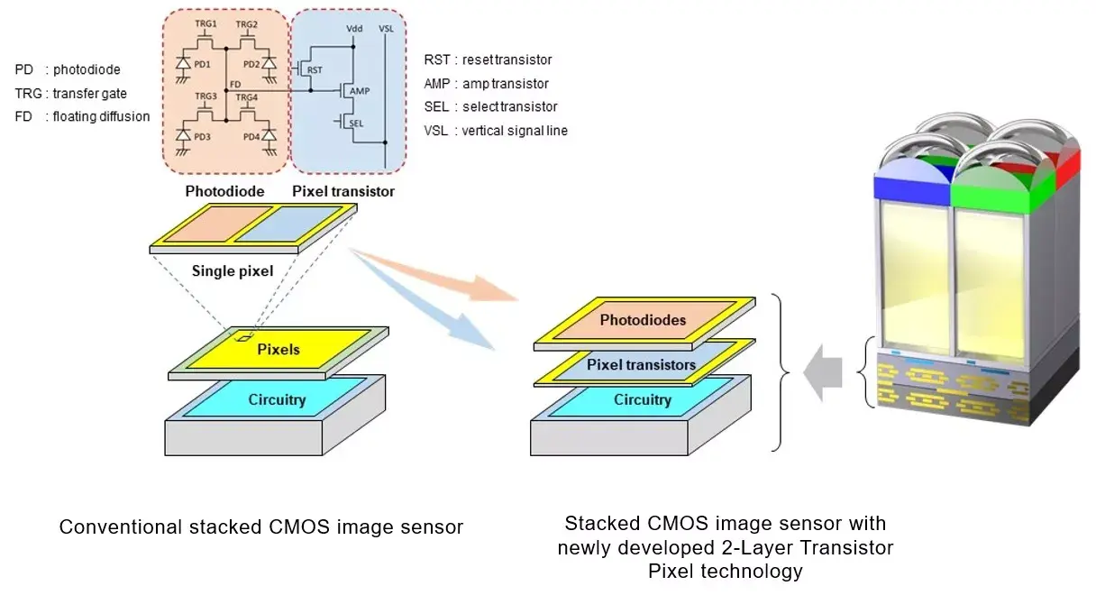
At the IEEE International Electron Devices Meeting, Sony announced its latest breakthrough in smartphone camera technology. Sony revealed the world's first stacked CMOS (Complementary Metal Oxide Semiconductor) image sensor with a dual-layer transistor pixel.
Sony's dual CMOS image sensor differs from traditional CMOS image sensors in that it has independent photodiodes and pixel transistors on separate substrate layers. A CMOS image sensor has a layered construction that includes a pixel chip with back-illuminated pixels stacked above a logic chip with signal processing circuits.
Unlike traditional CMOS image sensors, which have photodiodes and pixel transistors on the same substrate layer, Sony's innovative technology has photodiodes and pixel transistors on separate substrate layers.
Sony's new CMOS architecture technology optimizes the photodiode and the pixel transistor layers by doubling the saturation signal level and widening the dynamic range of an image. As a result, the imaging properties are significantly improved. The new pixel structure will allow pixels to maintain or increase their existing properties at both current and reduced pixel sizes.
Recommended For You
The new CMOS design enables Sony to increase the size of the amplifier transistors. With the increased size, Sony reduces the amount of noise that nighttime and other dark-location photos could have.
Sony's new CMOS technology will prevent underexposure and overexposure in situations with mixed lighting. Its latest image sensor design is promised to allow high-quality, low-noise photos even in low-light conditions.
Sony said that its new CMOS technology is intended for smartphones but did not provide a time frame when we could expect to receive phones using this new sensor design.
Get Visible as low as $20/mo for 1 year. Limited time offer with code: FRESHSTART
$20
/mo
$25
$5 off (20%)
Offer Ends 6.1.2026 at 11.59pm ET. New members get $5/mo off the $25/mg Visible plan, $35/mo Visible+ plan, or $45/mo Visible+ Pro plan for the first 12 months. Promo code FRESHSTART required at checkout.
Preslav Mladenov is a News and Affiliate Content Writer at PhoneArena who started on his tech journalism journey in December 2021. With persistent knack for finding the best deals out there, he swiftly became a pivotal Affiliate Content Writer, guiding readers towards significant savings on a plethora of gadgets, including smartphones, smartwatches, tablets, Bluetooth speakers, and headphones. Mladenov's deep-seated knowledge of mobile tech, paired with a rich background in sales, empowers him to unearth the finest deals on the web.
A discussion is a place, where people can voice their opinion, no matter if it
is positive, neutral or negative. However, when posting, one must stay true to the topic, and not just share some
random thoughts, which are not directly related to the matter.
Things that are NOT allowed:
Off-topic talk - you must stick to the subject of discussion
Offensive, hate speech - if you want to say something, say it politely
Spam/Advertisements - these posts are deleted
Multiple accounts - one person can have only one account
Impersonations and offensive nicknames - these accounts get banned
To help keep our community safe and free from spam, we apply temporary limits to newly created accounts:
New accounts created within the last 24 hours may experience restrictions on how frequently they can
post or comment.
These limits are in place as a precaution and will automatically lift.
Moderation is done by humans. We try to be as objective as possible and moderate with zero bias. If you think a
post should be moderated - please, report it.
Have a question about the rules or why you have been moderated/limited/banned? Please,
contact us.


Things that are NOT allowed:
To help keep our community safe and free from spam, we apply temporary limits to newly created accounts: