
President Biden gets a peek at Samsung's 3nm process node for next-gen chipsets
Samsung Foundry and TSMC are the two top independent chip foundries in the world. They take chip designs created by manufacturers like Apple, Qualcomm, Mediatek, Nvidia, and others and turn them into cutting-edge chipsets used on phones, automobiles, and other devices. Next year, both foundries will be shipping chips produced with the latest 3nm process nodes.
Typically the smaller the process node number, the higher the transistor count. And that is important because the higher the transistor count, the more powerful and energy-efficient a chip is. Besides moving to the next process node, Samsung will be using its latest transistor design known as Gate all-around (GAA) while TSMC will still be using the older FinFET design for its 3nm chips, also set to be included in some consumer devices (like the iPhone 14 Pro models) next year.
Samsung's 3nm chips will be up to 35% smaller, as much as 30% more powerful, and will consume up to 50% less energy
Using the 3nm process node with GAA is supposed to allow Samsung to deliver up to a 35% decrease in chip size, up to a 30% hike in performance, and as much as a 50% reduction in the use of energy. Today, Samsung was able to show off the new process node to U.S. President Joe Biden when he visited Samsung's campus earlier Friday. It is the world's largest semiconductor facility, according to Yonhap News (via Wccftech).
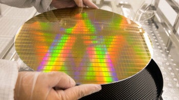
A wafer from which cutting-edge chipsets will be diced
Accompanying the president on his tour of the facility was Samsung Electronics Vice Chairman Lee Jae-yong. A Samsung official with knowledge of its advanced chip technology said, "Samsung could show a 3-nm chip to Biden to emphasize its foundry prowess over Taiwan's TSMC," Samsung did have an issue with poor yields on its 4nm production with reportedly only 35% of the chips it built at that process node able to pass quality control, about half of TSMC's yield at 4nm.
As a result, Samsung has lost some business to TSMC. The latter is building Qualcomm's Snapdragon 8+ Gen 1 chipset and is expected to produce the Qualcomm Snapdragon 8 Gen 2 Application Processor (AP). But previous reports have indicated that the yields on Samsung's 3nm GAA production have been even worse than its 4nm yield even though Samsung claims that its yields have been improving.
Samsung owns 18.3% of the global foundry business compared to TSMC's 52.1%
According to Trend Force, TSMC had a global market share of 52.1% in the industry during the fourth quarter of last year. Samsung's market share during the same time period was 18.3%. And looking ahead, Samsung is working on its 2nm process node and hopes to start mass-producing such chips by 2025.
TSMC is not likely to lose its lead over Samsung Foundry especially since Apple is its largest customer. Apple has already reserved 3nm chip production with TSMC for its A-series and M-series chipsets.

Popular stories


Latest News


Things that are NOT allowed:
To help keep our community safe and free from spam, we apply temporary limits to newly created accounts: