Qualcomm might count on TSMC to produce a 4nm Snapdragon chip next year
While Qualcomm designs the Snapdragon line of chips used by most Android phones, over the years they have been manufactured by TSMC and Samsung Foundry. Those are the two largest and most advanced contract foundries in the world. Samsung was responsible for the production of the 14nm Snapdragon 820 and the 10nm Snapdragon 835 and Snapdragon 845. The 7nm Snapdragon 855 was manufactured by TSMC before Qualcomm returned to Samsung for the 7nm Snapdragon 865 and this year's 5nm Snapdragon 888.
Qualcomm to reportedly leave Samsung and return to TSMC in 2022
Citing industry sources, Digitimes says that its next-generation 5G chip, dubbed the Snapdragon 895 for now, will be made once again by Samsung Foundry using the 5nm node. However, in 2022 Qualcomm will supposedly return to TSMC for a new chip that will be made using TSMC's 4nm process.
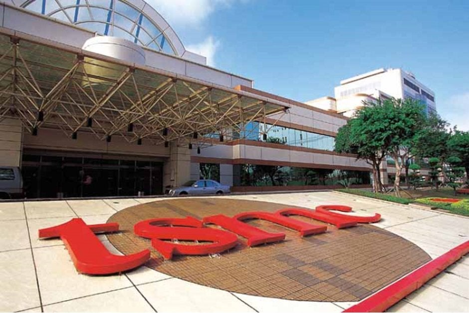
TSMC's chaorman says that the foundry is on track to produce 3nm chips in 2022
TSMC chairman Dr. Mark Liu has good news for those who follow Moore's Law. This is the observation made by Intel co-founder and former CEO Gordon Moore that calls for the transistor density on a chip (the number of transistors that fit inside a 2nm space) to double every other year. The higher the transistor density, the lower the process node, and the more powerful or energy-efficient a chip is. For example, 2019's A13 Bionic chip used on the iPhone 11 series was made using the 7nm node with a transistor density of 89.97 million transistors per square mm. The A13 Bionic contained 8.5 billion transistors. The A14 Bionic, used on the 5G iPhone 12 series, is manufactured using the 5nm node using a transistor density of 134 million transistors per square mm. The A14 Bionic is equipped with 11.8 billion transistors.
According to WccfTech, Dr. Liu says that the foundry's 3nm process node is right on schedule. Production is expected to start next year. Compared to the current cutting-edge 5nm process, the 3nm chips are expected to deliver an 11% gain in speed with a 27% reduction in power usage. The executive credited extreme ultraviolet (EUV) lithography for TSMC's shorter cycle times. EUV is able to create extremely thin patterns on wafers that are used to position the components used on a chip.
We also have some other TSMC news to tell you about. To make chips, a foundry needs plenty of water. However, Taiwan is suffering through a drought right now and the forecasts call for more of the same for the months ahead. Taiwan Water Company is calling this "the toughest moment." TSMC is ordering water by the truckload as the country widens its restrictions on water usage. Water levels are 20% below normal on the island after a lack of rain and the absence of a typhoon. Taiwan Economy Minister Wang Mei-hua told reporters yesterday, "We have planned for the worst. We hope companies can reduce water usage by 7% to 11%."
TSMC told Reuters that it has seen no impact on chip production. "We are making preparations for our future water demand," the world's largest contract foundry stated. Other foundries based in Taiwan have also have been dealing with the drought. Both Vanguard International Semiconductor Corporation and United Microelectronics Corp have inked pacts with water trucks and both also said that they have experienced no impact on production thus far.
Massive amounts of water are used in the production of chips. After each layer of semiconductors is added to a silicon wafer, the latter must be rinsed requiring the use of large amounts of water. To create an integrated circuit on a 12-inch wafer can require 2,200 gallons of water. Some of that water is Ultra Pure Water (UPW), thousands of times purer than drinking water. A Fab that processes 40,000 wafers each month can go through 4.8 million gallons of water each day. This equates to the annual water use for a city of 60,000 people.

Popular stories


Latest News


Things that are NOT allowed:
To help keep our community safe and free from spam, we apply temporary limits to newly created accounts: