TSMC starts constructing facilities to turn out 3nm chips by 2023

Powerful chipsets like the Qualcomm Snapdragon 855, Apple A13 Bionic and Huawei's HiSilicon Kirin 990 all have something in common. While designed by Qualcomm, Apple, and Huawei respectively, all three chips are actually manufactured by Taiwan Semiconductor Manufacturing Company (TSMC), the largest independent foundry in the world. And all three are produced using some variation of TSMC's 7nm process. That number indicates how many transistors fit inside an integrated circuit. The lower the process number, the higher the number of transistors inside a chip. The more transistors found inside a chip, the more powerful and energy-efficient it is. The number of transistors inside these components will blow your mind; the version of the Kirin 990 that features an embedded 5G modem carries over 10.3 billion transistors.
The process number has been shrinking for years. Back in the 1960s, Intel co-founder Gordon Moore observed that the number of transistors inside chips doubled every year. In the 1970s, this so-called Moore's Law was revised; the number of transistors inside these components would double every other year. That is a pretty hard task to accomplish, but TSMC plans to start 5nm production by next year. Samsung, which also runs a unit that manufacturers chips, will be producing 5nm chips next year as well. But at the beginning of next year, Samsung will use its 7nm EUV process to roll the yet to be announced Snapdragon 865 Mobile Platform off of the assembly line. EUV stands for extreme ultraviolet lithography, a technology that allows chip dies to be marked up more precisely, which allows more transistors to fit inside.
2021's Snapdragon 875 Mobile Platform, to be manufactured by TSMC, will most likely be the first 5nm chip found inside Android phones. As for Apple's A14, it is quite possible that TSMC will use the 5nm process to manufacture it. Remember, the 2020 iPhones won't be unveiled until late in the third quarter of next year. TSMC's Fab 18 will turn as many as 1 million wafers a month into 5nm chips once all three phases of the facility are completed by 2021.
Intel says that it will "recapture process leadership"
So what is happening beyond 5nm? We've already heard that both TSMC and Samsung have plans for 3nm production. Moore's Law has apparently not been rescinded. And ITHome is reporting that construction has already started on the fabrication facilities that TSMC will use for 3nm production starting in 2023. Covering over 74 acres of land in southern Taiwan's Science and Technology Park, the facilities will cost TSMC a reported $19.5 billion to build. Earlier in 2019, TSMC CEO C.C. Wei said that the development of 3nm was going smoothly. Samsung, for its part, plans on producing 3nm chips during the 2021-2022 time frame using its own next-generation GAA (Gate all-around) architecture. According to Tom's Hardware, Samsung's density won't be as high as TSMC's density for its 3nm process; this means that Samsung's chips at that node won't pack as many transistors into a small space as TSMC's will.
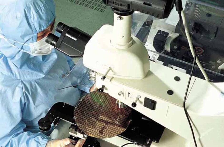
TSMC is spending a reported $19.5 billion to build the facilities needed to turn out chips using the 3nm process
Recently, Intel announced plans to "recapture process leadership" even though it just started turning out 10nm Ice Lake-U mobile processors. Intel CEO Bob Swan says, "We are accelerating the pace of process node introductions and moving back to a two to two-and-a-half year cadence. Our process technology and design engineering teams are working closely to ease process design complexity and balance schedule, performance, power and cost." This would require Intel to really make up for lost time as it had trouble getting to 10nm. Intel could be considered a year or so behind TSMC and Samsung right now. As a matter of comparison, 2018's Snapdragon 845 Mobile Platform was built using the 10nm process.
While Moore's Law was once considered dead at 5nm, obviously this does not appear to be the case. TSMC is said to be looking at stacking transistors vertically as a way to pack more inside chips and is reportedly researching the periodic table to find materials for the packaging of future chips.

Popular stories


Latest News


Things that are NOT allowed:
To help keep our community safe and free from spam, we apply temporary limits to newly created accounts: