History is made! Samsung beats out TSMC and starts shipping 3nm GAA chipsets

For the time being, Moore's Law, the observation made by semiconductor legend Gordon Moore, remains alive. Moore, the co-founder of Fairchild Semiconductor and Intel, originally noted in 1965 that the number of transistors inside an integrated circuit (IC) would double every year. He later revised that in the 1970s by stating that the transistor count would double every other year.
The process node used by top foundries like TSMC and Samsung for building cutting-edge chips gives us an idea of how Moore's Law is doing. The smaller the process node, the larger the number of transistors that can fit inside an IC. And that is important because the higher the transistor count, the more powerful and energy-efficient a chip is.
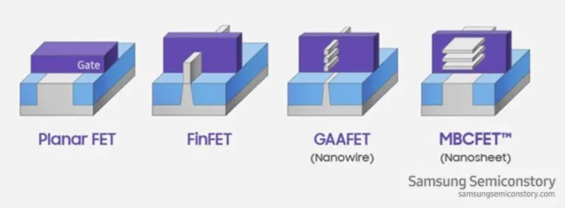
Samsung started shipping its 10nm SoCs in 2016. In 2018 it started mass production of its 7nm chipsets. By 2020, Samsung started mass production of 5nm chipsets, and now Samsung (via wccftech) has become the first to start shipping 3nm GAA chipsets beating out rival TSMC. Not only is Samsung the first to deliver 3nm chips, but it is also the first to ship these chips equipped with GAA or gate-all-around transistors.

Samsung is the first to start shipping 3nm GAA chipsets which replaces the previous generation 5nm FinFET chips
With GAA, there is more control over current flow resulting in greater power efficiency. TSMC is still using the previous generation FinFET transistor design for its 3nm SoCs which it will start shipping during the second half of this year. The world's leading independent foundry will start using GAA with its 2nm process node which it hopes to start delivering to customers in 2026.
Samsung was so stoked to beat out TSMC with its 3nm deliveries that the company held a ceremony at its Hwaseong Campus, in Gyeonggi-do, which was attended by several Samsung executives and Korean politicians. The first batch of 3nm SoCs are not being shipped to smartphone manufacturers. Instead, they will be used in equipment employed by cryptocurrency miners, with the new 3nm GAA allowing for a big reduction in power consumption.
Eventually, the 3nm GAA process node will be used to produce smartphone chips including Samsung's own Exynos 2300 and possibly the Qualcomm Snapdragon 8 Gen 2 SoCs. The 3nm GAA process node will reduce power consumption by up to 45% and increase performance by as much as 23% when compared to the 5nm node. A second generation variant of the 3nm GAA chips is expected to reduce energy consumption by up to 50%, and increase performance by up to 30%.
What this will mean to you is the availability of more powerful handsets with improved battery life.
In a release, Samsung said, "On the 25th, Samsung Electronics held a 3nm foundry product shipment ceremony using next-generation transistor GAA (Gate All Around) technology at the V1 line (EUV only) at Hwaseong Campus, Gyeonggi-do. The event was attended by about 100 people including Minister of Trade, Industry and Energy Changyang Lee, suppliers, fabless, Samsung Electronics DS division head, Kyeong-hyeon Kye (President), and executives and employees, and encouraged executives and employees who participated in 3nm GAA R&D and mass production."


Things that are NOT allowed:
To help keep our community safe and free from spam, we apply temporary limits to newly created accounts: