TSMC will start the mass production of its next-gen cutting-edge chips this week
The world's largest chip foundry, TSMC, is about to kick off mass production of cutting-edge chips using its 3nm process node. To put it in simple terms, as the process node number drops, the transistors used to build these integrated circuits become smaller allowing more of them to fit inside a small, dense space like a chip. And the higher a chip's transistor count, the more powerful and energy-efficient it is.
For example, the A13 Bionic used to power 2019's iPhone 11 series was produced using TSMC's enhanced 7nm process node. That SoC carried 8.5 billion transistors. This year's A16 Bionic was manufactured by TSMC using its 4nm process node and sports nearly 16 billion transistors. Next year's A17 Bionic is expected to roll off of TSMC's assembly lines having been built with TSMC's enhanced 3nm process node (we will return to that soon).
The iPhone 15 Pro and iPhone 15 Ultra are expected to feature the 3nm A17 Bionic chipset
Apple is TSMC's largest customer and it is responsible for 25% of the company's revenue. Digitimes (via MacRumors) writes that this week, TSMC is expected to start mass production of components using the 3nm process node; before the A17 Bionic finds its way into the iPhone 15 Pro and iPhone 15 Ultra, Apple might place its 3nm M2 Pro chip into the MacBook Pro and the Mac Mini.
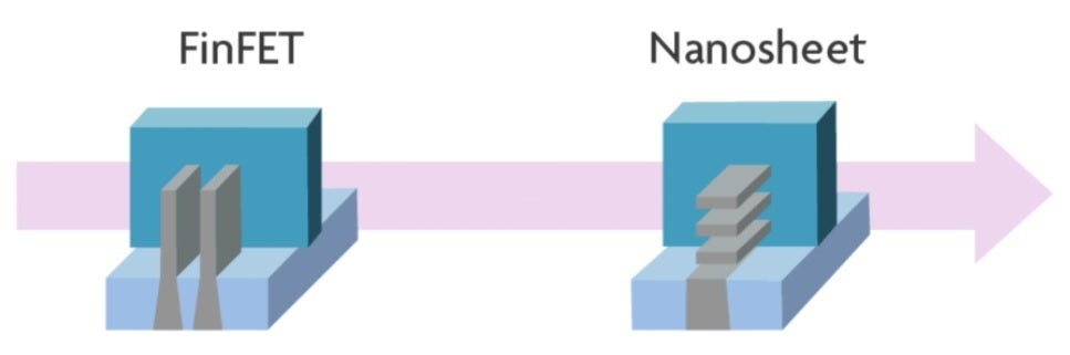
TSMC's 3nm chips will continue to use FinFET transistors (at left) while Samsung's 3nm chips will use GAA
This Thursday, TSMC is expected to mark the beginning of 3nm mass production by holding a ceremony at Fab 18 at the Southern Taiwan Science Park. At the event, TSMC will discuss its plans to expand 3nm production at that fab. The A17 Bionic and the M3 chip are both expected to ship later next year having been built using TSMC's enhanced 3nm process node.
The only other foundry in the world able to mass produce at 3nm presently is Samsung Foundry. The latter uses gate-all-around (GAA) transistors which allow for more precise control of current flow through each transistor. This is accomplished by having the gates (which turn on and off to allow or block current flow) come into contact with the channels on all sides. With GAA, power efficiency is improved. Simply put, chips using GAA transistors run faster and consume less power than chips using FinFET transistors.
Samsung to use GAA transistors with its 3nm production; TSMC will continue with FinFET until it's at 2nm production
While Samsung is using GAA for its 3nm chips, TSMC won't use it until it hits 2nm production which could be in 2025. TSMC will continue to employ FinFET transistors on its 3nm chips which cover only three sides of the channel. The main difference between FinFET and GAA is that the former uses horizontally placed "fins" to increase electricity flow. With GAA, vertically stacked nanosheets are used instead. The placement of the wide nanosheets also reduces current leakage (thus requiring less power) and improves current drive.
Intel, which says that it will soon challenge TSMC and Samsung for process leadership in a few years, will also use GAA starting in 2024. Intel calls its GAA transistors RibbonFET. The U.S.-based chipmaker said earlier this month that it hopes to be able to fit one trillion transistors into a single package by 2030.
So what's coming after 3nm?
So what is coming up next? As we mentioned, TSMC and Samsung Foundry are expected to produce 2nm chips as soon as 2025 with Samsung Foundry's roadmap calling for it to ship 1.4nm chips starting in 2027. TSMC hasn't really discussed what it will do after 2nm except that it did briefly mention a 1nm process node.
Helping with Intel's quest to topple TSMC and Samsung Foundry, it will be the first foundry to own ASML's next-generation Extreme Ultraviolet (EUV) lithography product, the High Numerical Aperture Extreme Ultraviolet Lithography machine. ASML is responsible for the production and sale of every EUV lithography machine on the planet.
The new lithography machines will allow foundries to etch circuitry designs at higher resolutions to enable 1.7x smaller chip features and 2.9x increased chip density. This will help Intel etch extremely thin circuity patterns on wafers allowing for the placement of billions of additional transistors to be placed inside a chip.
TSMC also announced earlier this month that it will produce some 3nm chips at a second fab it is building in Arizona. Apple CEO Tim Cook said that the company will buy an undisclosed amount of those components.

Popular stories


Latest News


Things that are NOT allowed:
To help keep our community safe and free from spam, we apply temporary limits to newly created accounts: