Key Apple and iPhone supplier reveals stunning roadmap taking us through 2027

Before chip foundries could start producing chips using process nodes under 7nm, the extreme ultraviolet (EUV) lithography machine had to be invented. The machine etches circuitry patterns thinner than human hair on silicon wafers which allows billions of transistors to be shoehorned inside a single chipset. For example, each A17 Pro application processor inside the iPhone 15 Pro models carries 19 billion transistors.
The lower the process node, the smaller are the transistors used with a chip meaning that the transistor count can be higher. Typically the higher the transistor count, the more powerful and energy-efficient a chip is. There is one company in the world, Dutch firm ASML, that makes EUV machines and it has been promoting and selling the next-gen device. This is called the high-NA EUV machine and thanks to a hike in the numerical aperture to .55 from .33, more precise patterns can be etched on wafers that will be used to produce chips using the 2nm process node and lower.
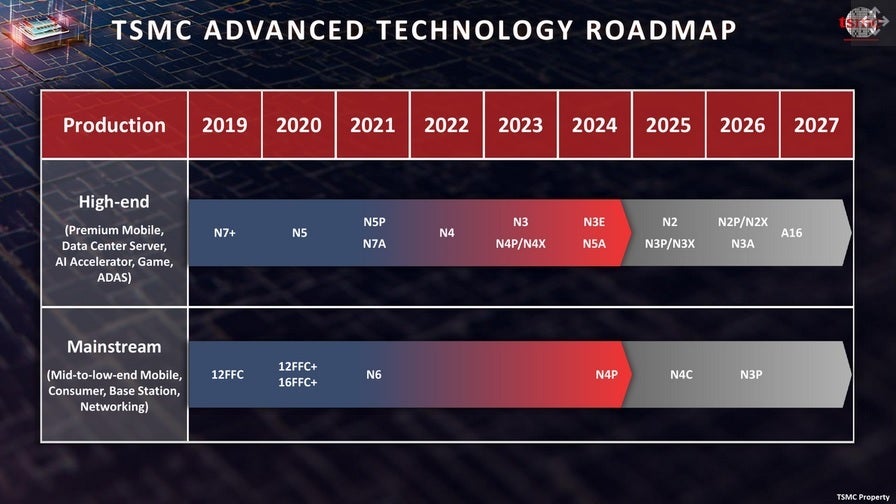
TSMC's roadmap. | Image credit-TSMC
Earlier this year a video was released showing the first high-NA EUV machine being installed by Intel as the latter was the first chipmaker to buy the $400 million machine. Today we've learned that the world's largest foundry, TSMC, is expected to have its first high-NA EUV machine installed at its Hsinchu R&D center by the end of the year. While TSMC at first refused to discuss whether it would purchase one of the second-gen EUV lithography machines, it now has gone full steam ahead as the company plans to keep its title as the world's largest contract foundry by continuing to have process leadership.
"The roadmap you see here is pretty much the same, actually it is the same technology roadmap that I think you saw during the [technology] symposium six months ago. We have N2, N2P, which is coming [to] productions next year and the year after. And then [they are] followed by A16."-Dan Kochpatcharin, Head of Design Infrastructure Management, TSMC
Additionally, TSMC says that its 1.6nm node is on track to start mass production in 2026 and it will start to use the high-NA EUV machine in order to manufacture chipsets at 1.4nm in 2027. TSMC's 2nm node (N2, N2P, N2X), and 1.6nm node will use Gate-All-Around transistors which employ vertically placed horizontal nanosheets allowing the gate to cover the channel on all four sides. This reduces current leaks, improves the drive current, and offers higher performance with improved energy efficiency.
The A16 uses a backside power delivery network (BSPDN) that moves the wires and connections that feed a chip with power from the front of the chip to the back which will improve performance efficiency.












Things that are NOT allowed:
To help keep our community safe and free from spam, we apply temporary limits to newly created accounts: