To alleviate the global chip shortage, TSMC considers building a new factory in Singapore

According to The Wall Street Journal, TSMC, the world's largest independent foundry, is considering spending billions of dollars in order to build a new fabrication facility in Singapore. With the current chip shortage, TSMC needs to add production capacity to make sure that it can deliver enough cutting-edge chipsets to meet demand from its top customers including Apple, Qualcomm, and Mediatek.
TSMC negotiating to build a new fab in Singapore to alleviate the global chip shortage
The report from The Journal says that TSMC has not yet made a final decision about proceeding with a new fab and the factory being built in the U.S. (in the state of Arizona) is currently delayed. A new plant in Singapore would cost billions of dollars and some of the money to build the facility could come from the Singapore government. Those in the know say that TSMC is currently in negotiations with the country's Economic Development Board.

Render of TSMC's Arizona fab that is now being delayed
A TSMC spokesman says, "TSMC doesn’t rule out any possibility but does not have any concrete plan at this time." TSMC and Samsung Foundry are the top two independent foundries in the world which means that manufacturers send their chip designs to them to be built. For example, Apple designs its A-series and M-series SoCs and turns over the manufacturing of the components to TSMC. Apple, in fact, is that foundry's largest customer.
Both TSMC and Samsung will start shipping chips made using their 3nm process nodes in time to have them included in consumer products next year. The smaller the process node number, the larger the number of transistors that can be found inside a chip. This is important because the larger the number of transistors in a chip, the more powerful and energy-efficient it is.
For example, the A13 Bionic chip powered the iPhone 11 series was built by TSMC using its 7nm process node. The chip contained 8.5 billion transistors. Compare that with the A15 Bionic chip built by TSMC using its 5nm process node. That chip, used on the iPhone 13 line, carries 15 billion transistors allowing it to be more powerful and energy-efficient than older chips.
The now-delayed fab being built in Arizona was aiming to produce 5nm chips by 2024. That factory would not be shipping cutting-edge chipsets since by 2024 TSMC's Taiwan-based fabs should be churning out 3nm chips. The proposed Singapore factory would make 7nm to 28nm chips and these older production technologies turn out chips used for smartphones, automobiles, and other devices.
Ironically, during the current global chip shortage, it has been these older legacy nodes that have been in short supply and have risen the most in price. But building fabs in other countries could help TSMC remain close to its major customers and is a way around some of the travel restrictions that come companies have imposed due to COVID. Last year Global Foundries announced that it would spend $4 billion to build a fab in Singapore that would open in 2023.
Singapore is responsible for 5% of global wafer fabrication
Singapore is already home to several chip suppliers as it has a large talent pool that these companies can choose from, and it has a strong supply chain. U.S. chipmaker Micron Technology, Germany's Infineon Technologies, and Global Foundries have facilities in the country. The country's trade and industry minister Alvin Tan said in January that semiconductors are "the fastest-growing segment of the electronics industry."

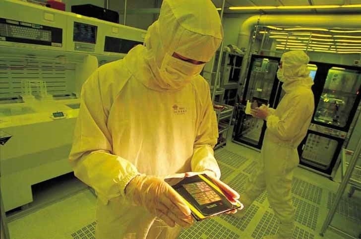
TSMC employee checking things out in a fab
Earlier this year, back in February, the world's fourth-largest contract chip manufacturer, Taiwan’s United Microelectronics Corp., said that it would spend $5 billion to expand its production in Singapore. The latter country is home to 5% of global wafer fabrication capacity. Wafers are made of silicon and through various techniques they are turned into an ingot. The ingots are then sliced into thin discs called wafers on which extremely thin circuity patterns are etched in a process known as lithography.
After being polished to a mirror finish, the wafers go through several stages and cut into dies. They are then tested, packaged, and shipped.
Follow us on Google News


Things that are NOT allowed:
To help keep our community safe and free from spam, we apply temporary limits to newly created accounts: