Samsung's new chip factory will help it compete with TSMC
Taiwan Semiconductor Manufacturing Company (TSMC) is the world's largest contract foundry. The company churns out chips designed by Apple, Huawei (until September 14th), Qualcomm, and others. Can you name the second-largest contract foundry worldwide? If you said Intel, you answered incorrectly; the company only produces chips for itself. Actually, the independent foundry looking up at TSMC is Samsung.
Samsung's new fab will churn out 5nm chips late next year
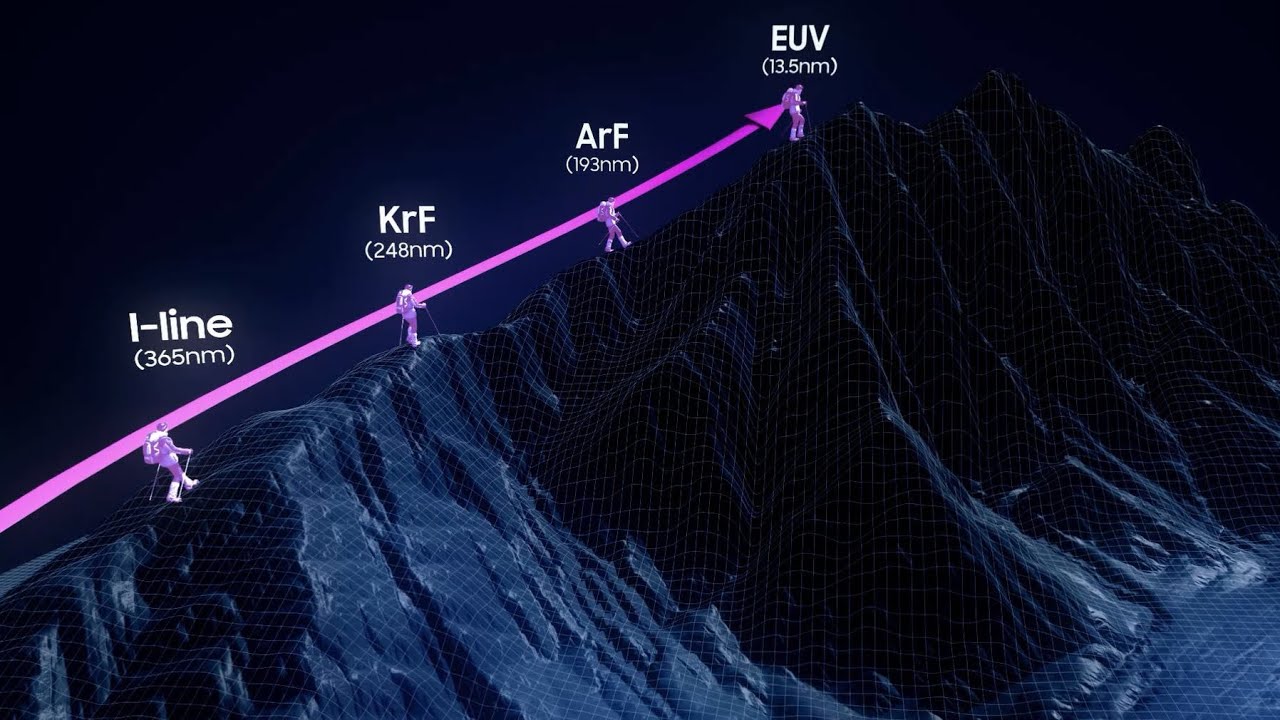
Both TSMC and Samsung are currently the only contract foundries that can ship chips made using the 10nm process node and lower. This number is based on transistor density and both are expected to deliver 5nm chips this year with 171.3 million transistors packed in each square mm. That is important since the higher the number of transistors in a chip, the more powerful and energy-efficient it is. The 2020 5G iPhone 12 family, powered by the A14 Bionic chipset, could well be the first smartphones to be powered by a 5nm SoC. Since the U.S. Commerce Department is allowing Huawei to receive chips made from wafers currently in production for 120 days, later this year the Huawei Mate 40 series will use a 5nm Kirin chipset under the hood (after the 120 days is up, TSMC will need an export license from the U.S. to ship to Huawei). Samsung will produce 5nm EUV (more on that below) chips in the second half of this year from its Hwaseong fab.
So 5nm is currently the cutting-edge process node and Samsung has started construction of a new factory that will help it spit out more 5nm chips. The fabrication facilities are being constructed south of Seoul in Pyeongtaek and will use Extreme Ultraviolet Lithography (EUV) to mark up a wafer. This technology creates patterns on the wafer that shows the positioning of transistors. Using extremely thin ultraviolet beams, EUV can mark up a wafer with room for more transistors. The new factory will greatly increase Sammy's EUV production capabilities.

Samsung owns the second-largest independent foundry in the world.
Samsung says that the 5nm EUV chips from this plant will be used in 5G networks and high-performance computers by the second half of 2021. The fab will also be used to manufacture 3nm chips once the company moves on to mass production of the next lower process node. The transistor density of these chips will reach an amazing 300 million per square mm.
Dr. ES Jung, President and Head of Foundry Business at Samsung Electronics, says, "This new production facility will expand Samsung’s manufacturing capabilities for sub-5nm process and enable us to rapidly respond to the increasing demand for EUV-based solutions. We remain committed to addressing the needs of our customers through active investments and recruitment of talents. This will enable us to continue to break new ground while driving robust growth for Samsung’s foundry business."
With the new facilities, Samsung will own seven foundry production lines in the U.S. and South Korea. TSMC announced late last week that it will build a $12 billion fab in the U.S. that won't be running until 2023. The factory will produce 5nm chips at a time when the industry could be moving to 3nm. As a result, the announcement by TSMC really doesn't change anything since the U.S. will still need to obtain 3nm chips overseas come 2023. Besides, the Arizona facility will produce only 20,000 wafers a month; that's a drop in the bucket compared to the 12 million wafers produced by TSMC in 2019. But unlike Samsung's new factory in Seoul, TSMC's plant in Arizona is really about creating jobs for Americans.
In April, TSMC said that it had started research and development on 2nm chips. We could see that process node in massproduction as soon as 2025 with a transistor density (mind you, this is just an estimate based on recent performance) of 520 million to 540 million transistors per square mm.

Popular stories


Latest News


Things that are NOT allowed:
To help keep our community safe and free from spam, we apply temporary limits to newly created accounts: