
Undisclosed foundry is the second buyer of ASML's $400 million second-gen EUV machine
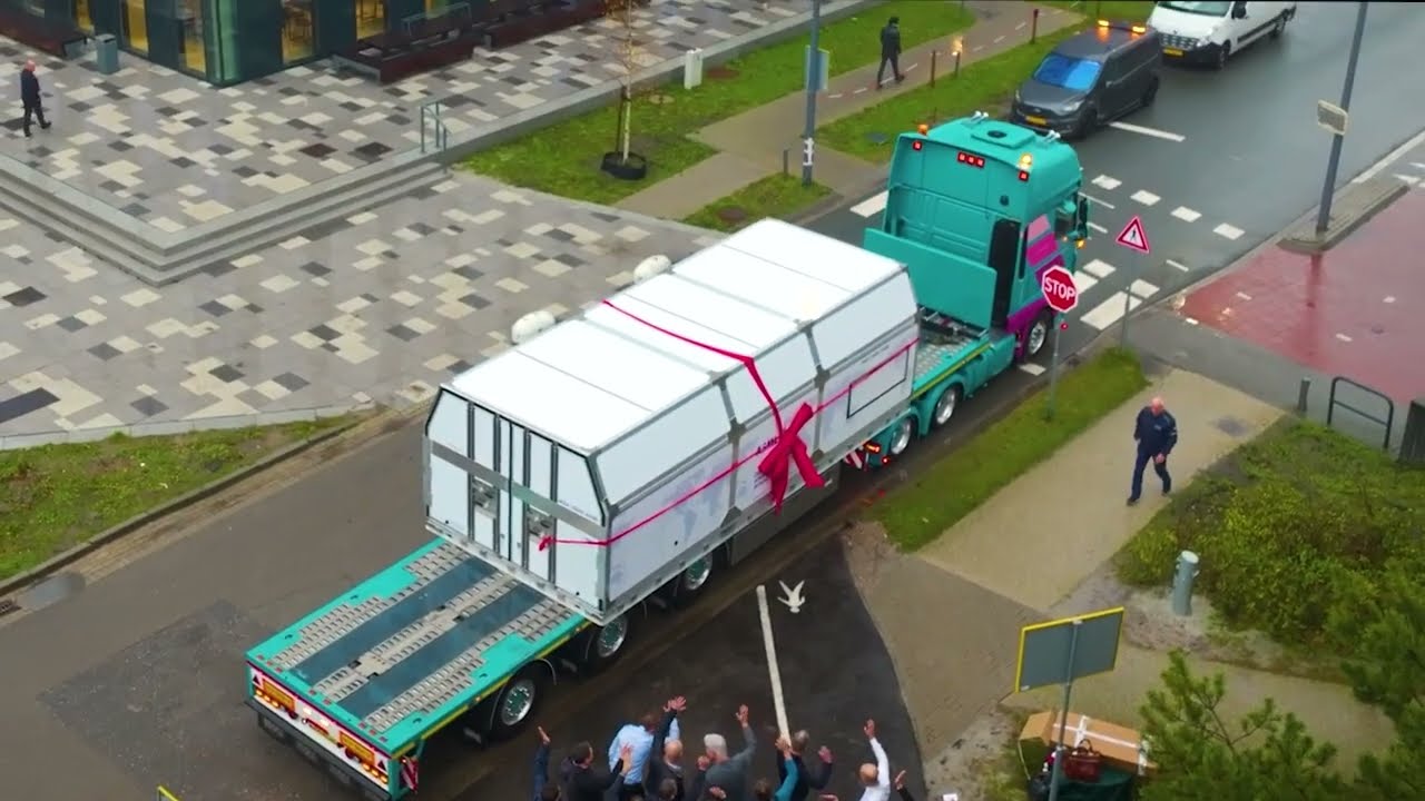
Last December, Dutch tech firm ASML shipped its first second-generation Extreme Ultraviolet Lithography (EUV) machine to Intel. ASML is the only company in the world that makes the EUV machines that etch complex circuitry patterns on silicon wafers to help foundries properly place billions of transistors inside the small chipsets that drive smartphones. The second-gen High-NA EUV machines have an aperture of .55, equivalent to a resolution of 8nm. First-gen EUV machines have an aperture of .33, equivalent to a resolution of 13nm.
With a higher-resolution pattern transferred to a wafer, a foundry might not have to run a wafer through the EUV a second time to print the details needed which saves the foundry both time and money. At ASML's conference call following its latest earnings report, Christophe Fouquet, chief business officer of ASML, said, "Regarding High-NA, or 0.55 NA EUV, we shipped our first system to a customer and this system is currently under installation. We started to ship the second system this month and its installation is also about to start."
The recipient of the second High-NA EUV to ship is unknown. TSMC, the world's largest foundry, is probably not the unnamed buyer of the latest High-NA EUV to be ordered. The foundry will have to buy one sometime, but it doesn't seem that it is interested in making this purchase now. Meanwhile, ASML is believed to be working on the third-generation Hyper-NA EUV with a numerical aperture above .7.
Intel is in the process of installing its Twinscan EXE:5000 High-NA EUV which cost the company about $400 million. Intel will start using the machine when it begins producing chips with its Intel 14A process node. By getting a head start on installing and using the machine, Intel might grab an advantage in an upcoming three-way battle for process leadership between Samsung Foundry, TSMC, and Intel. Intel's 14A process node, equal to TSMC and Samsung's 1.4nm process nodes, is expected to be used in mass production sometime in 2027 around the same time that TSMC and Samsung Foundry kick off 1.4nm production.
When process nodes decline, so does the size of the transistors used with these chips. That means more transistors can fit inside these components and the higher a chip's transistor count, the more powerful and/or energy-efficient a chip is. That's why the High NA EUV is so important. As process nodes shrink and more transistors fit inside chips, the circuitry patterns etched on the silicon wafers need to be made using a finer resolution in order to shoehorn billions of transistors inside these components.
ASML's Fouquet says, "The customer interest for our [High-NA] system lab is high as this system will help both our Logic and Memory customers prepare for High-NA insertion into their roadmaps. Relative to 0.33 NA, the 0.55 NA system provides finer resolution enabling an almost 3x increase in transistor density, at a similar productivity, in support of sub-2nm Logic and sub-10nm DRAM nodes."

Popular stories


Latest News


Things that are NOT allowed:
To help keep our community safe and free from spam, we apply temporary limits to newly created accounts: