
Battle between two companies will uphold the "law" that will lead to more powerful smartphones

Two of the top foundries in the world belong to Taiwan Semiconductor Manufacturing Company (TSMC) and Samsung. The former is the world's largest independent foundry which means that it manufactures chips for companies like Apple and Huawei that design their own components, but do not have the facilities to fabricate them. TSMC is supposed to host a press conference in April during which it will release more details of its roadmap to 3nm chip production.
The process node references the number of transistors that fit inside an integrated circuit. The smaller the process node, the larger the number of transistors inside a chip. For example, the 7nm Kirin 990 5G, manufactured by TSMC for Huawei's HiSilicon unit, is packed with more than 10.9 billion transistors. A chip with more transistors inside is more powerful and energy-efficient. The 5nm Apple A14 Bionic will reportedly be equipped with 15 billion transistors; TSMC will be churning out 5nm chips starting in the second half of this year and among the first chips at this process node will be the A14 Bionic and Huawei's next flagship chip expected to be called the Kirin 1020.
You can imagine how many transistors will be packed inside 3nm chips. At this stage, only TSMC and Samsung have a roadmap to get there. According to MyDrivers, at the Samsung Foundry Forum held in Japan last year, the company said that its 3nm chips will provide 35% improved performance compared to 7nm chips (like the Exynos 990 which will be used in the European Galaxy S20 line in Europe) and cut power consumption by 50%. Samsung hopes that at 3nm it will become the largest foundry in the world. Samsung says that it will be able to start mass production of 3nm chips as soon as next year. TSMC has invested $19.5 billion in a factory that will turn out 3nm chips and construction of the facility will start this year.
Samsung is dropping the use of FinFET transistors to get to 3nm
To get to 3nm, Samsung has dropped the use of its FinFET transistors and instead is using its MBCFET (Multi-Bridge-Channel FET, multi-bridge-channel field effect tube) technology to improve transistor performance. It also is compatible with the FinFET manufacturing process which will make it faster and easier for Samsung to make the move to 3nm. TSMC still will have to decide whether to continue using FinFET transistors or move to Gate-All-Around (GAA) transistors as Samsung has.
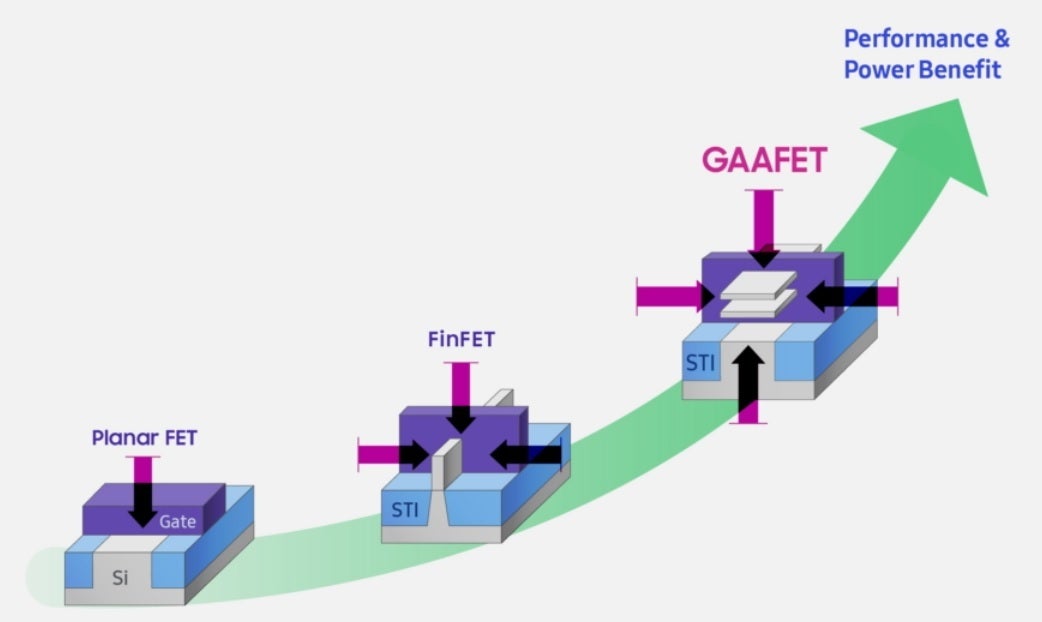
Samsung is dropping FinFET transistors and will use GAA to get to the 3nm process node
At stake is the continuation of the observation known as Moore's Law. Discovered by Intel co-founder Gordon Moore, the original observation called for the number of chips inside an integrated circuit to double every year. In 1975, 10 years after he first made the observation, Moore revised his "Law" calling for the number of transistors inside an integrated circuit to double every other year. Over the years, tech analysts have constantly called for the death of Moore's Law but TSMC and Samsung have kept it alive with the use of technology like extreme ultraviolet lithography. The latter uses ultraviolet light to mark up more precise patterns on a silicon wafer; since these patterns show where transistors will be placed inside a chip, the ability to mark up these patterns more precisely allow for the placement of more transistors inside.
To give you an example of the progress made by the industry over the years, the first SoC designed in-house by Apple was the A4 which debuted on the OG iPad and the iPhone 4. The component was built using the 45nm process and as we previously pointed out, 2020's A14 Bionic will be manufactured using the 5nm process node.
This April, when TSMC discusses the 3nm process node with the press, we should learn much more about the foundry's roadmap to 3nm, 2nm and perhaps even lower.

Popular stories


Latest News


Things that are NOT allowed:
To help keep our community safe and free from spam, we apply temporary limits to newly created accounts: