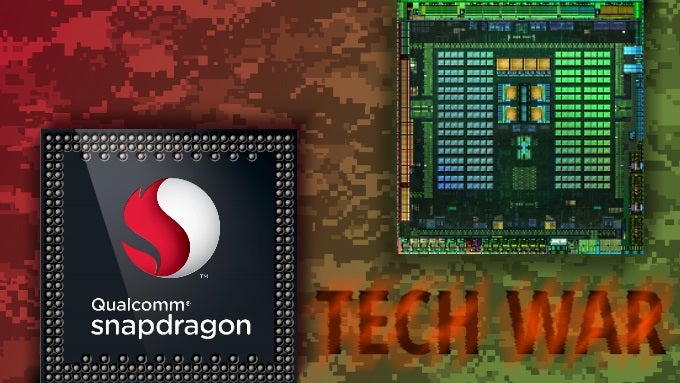
Tech war: Nvidia Tegra X1 takes on Snapdragon 810 with raw GPU power
CEO Huang announces the Tegra X1
Central processing units (CPU)
So, technically, it's almost the one and the same CPU, huh? No, it's not. The similarities end here. There's a multitude of differences in optimization techniques, turbo & throttling management, and built-in technologies to differentiate the X1 and 810. Most importantly, their graphics units are totally different.
Graphics processing units (GPU)
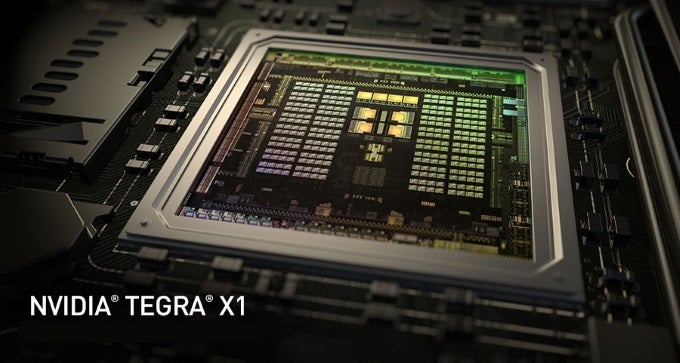
The Tegra X1 continues Nvidia's strategy of scaling down its general-purpose GPU microarchitecture to a mobile format. It took two years for the Kepler m-a, which debuted in the company's GeForce 600 series of desktop cards, to reach Nvidia's mobile computing projects. For the Tegra X1, it took the company just one year to introduce its Maxwell m-a to a mobile GPU - cheers for progress! Talking about progress, the Tegra X1's GPU escalates to a whopping 256 shader cores, up from the no-less impressive 192 shader cores found in its predecessor's.
Impressed? Wait until you see what Qualcomm did with the Adreno 430 GPU that bosses the Snapdragon 810's graphics department. This beast has 288 shader cores - more than the Tegra X1 ever had! You might have missed that, because unlike Nvidia, Qualcomm simply didn't market it to you. But really, it's not only the quantity that matters here, it's how hard they're being pushed. The Tegra X1's GPU clock speed reaches a whirring 1GHz, while the Adreno 430 purrs at 600MHz. The last factor alone is enough to let the X1 claim the raw GPU power crown, but it is not that simple in reality.
See, Nvidia designed the X1 for car computers first. It has all that power so it can calculate distances and maneuvers on the fly while processing video signals from up to six cameras, simultaneously. Of course, the chipset can play 3D games like it invented them, but its full potential can be harnessed only in the setting of a modern vehicle. If the chip ended up in a tablet ot smartphone, it would have to be throttled down to clock frequencies that ensure the chip won't be an overheating battery drain. Unless liquid cooling and double capacity battery packs turn reality overnight, the X1 in a smartphone or tablet won't be mind-blowingly faster than today's premium processors.
Connectivity and multimedia technologies
Now that we've examined the hardware thoroughly, let's see the additional features these SoC's are enabling. Smartphones and tablets are multimedia and connectivity powerhouses, first and most, so there's a heavy emphasis on fast internet and high-resolution video. Thus, the Nvidia X1 is ready to power 4K displays or feed 4K@60fps content to an external display over HDMI 2.0. It supports H.265 and H.264 encoding and decoding, while JPEG de/compression boasts a 5x speed boost. eMMC 5.1 storage support is also included. Connectivity-wise, the X1 hasn't been properly detailed yet, but we can assume it will have the BT, Wi-Fi, NFC, GPS, 2G/3G/4G bases covered.
Is the Tegra X1 really more powerful than a supercomputer?
Nvidia advertised the X1 as the first mobile chip that's more powerful than a supercomputer. Here's what the company said, verbatim:
“Tegra X1 packs more power than the fastest supercomputer of 15 years ago, ASCI Red. Run for 10 years by the U.S. Department of Energy’s Sandia National Laboratory, ASCI Red was the first teraflops (FLOPS – floating point calculations per second) supercomputer system. ASCI Red occupied 1,600 square feet and gulped 500,000 watts of power. By contrast Tegra X1 sips less than 15 watts of power.”
Is it really so?
That's not a locker room. It's the first teraflop supercomputer!
The short answer is “not quite.” The long, scientific answer is that the super-computer story is great for marketing, but computer tech website KitGuru's super-computations prove the reality is quite different:
“Nvidia's PR technologists decided to compare FP16 (16-bit floating point) performance of Tegra X1 to FP64 (64-bit floating point) performance of ASCI Red supercomputer, the world’s first 1TFLOPS supercomputer. The problem is that while FP16 is enough for certain graphics applications today (still, loads of apps use full FP32 precision), it is definitely not enough for any kind of high-performance computing applications. So, comparing FP16 performance to FP64 performance is clearly an apples to oranges kind of comparison. But an important thing is that Maxwell architecture was not designed for supercomputers, its FP64 rate is about 1/32 of its FP32 rate. So, if 256 SPs inside the Tegra X1 can offer 512GFLOPS at FP32, then its FP64 rate is 16GFLOPS. Not quite a teraflop, eh?”
That's the cold mathematical proof Nvidia's marketing probably didn't want you to see. However, credit has to be given where it's due – at FP16 operations, the Tegra X1 nails a peak 1024 GFLOPS, a full teraflop of processing power. This probably fueled the “supercomputer” angle of the announcement, and it does make for an incredibly powerful processor, hands down.
Conclusion
The Nvidia Tegra X1 is the most advanced SoC for mobile applications by far. Yet, the company explicitly stated that the kind of power it enables is not needed in today's smartphones and tablets, but for self-driving cars. Outside the automotive industry, we expect to see a limited number of mobile devices use the X1 in an underclocked form, at best. Thus, Nvidia's beast isn't a threat to Qualcomm's hegemony over the mobile chipset industry. The Snapdragon 810 remains the one processor you'll be seeing in most flagship smartphones and tablets for the majority of 2015, and Nvidia is okay with that, because it's after a different market with the X1.


Things that are NOT allowed: