Besides Samsung, Apple's foundry darling TSMC is the main challenger in the battle for leadership in the production of chips using the upgraded 7nm process. Last fall, Samsung announced that it is kickstarting a new chipset method production, and we will spare you all the juicy argon fluoride against ultraviolet details, going straight to the benefits for the end user.
Chips made with the second-gen 7nm extreme ultraviolet (EUV) lithography can be produced easier, with better yields, and with a reduced number of masks needed for production that will make them cheaper to make on average. At the same time, compared with the 10nm chips in the Note 9 or iPhone X, the EUV silicon can be made with a 40% smaller footprint, and either 20% faster, or with the whopping 50% reduction in power draw.
Samsung's chief of the semiconductor LSI division called the technology "challenging" during the quarterly results press conference, yet mentioned that Samsung expects to become a leader there. Why? Well, it thought it will be the exclusive producer of second-gen 7nm chipsets, made with the EUV equipment that helps laying down the minuscule transistors close to each other without too much drama.
It turns out, however, that TSMC didn't rest on its laurels and, while it made Apple's A12 chipset in the iPhone XS with the first-gen 7nm process, the A13 will be done with the 7nm EUV method, and it has already entered mass production. Thus, unless Samsung releases the Note 10 with a different processor than those in the Galaxy S10, the 2019 iPhone may be the first to use a 7nm+ processor.
Recommended Stories
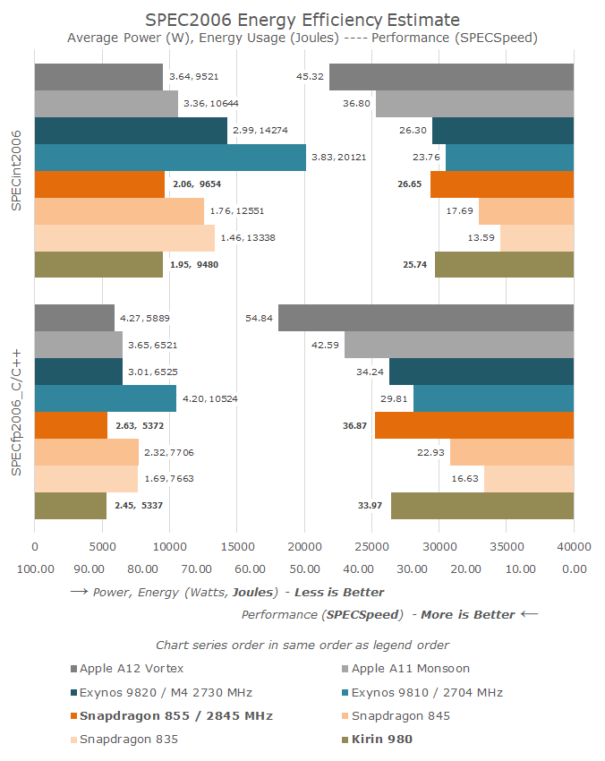
This will most likely result in all the performance and power draw superiority we've come to expect from its A-line chips, as this Anandtech chart below shows. Note that Apple A12 offers more oomph at the same power draw compared to the competition.
Since today's mobile processors are powerful enough, we'd wager to guess that the designers of the future AX Bionic, Snapdragon, or Exynos chipsets, will opt for a diminished toll on battery life, and the space saved by the EUV method will be utilized for something else in the increasingly crowded smartphone internals.
TSMC also announced that it is sampling the 5nm EUV process which should become available for production in the first quarter of 2020 or just around the time of Android's spring flagships. Could the Snapdragon 865 jump directly into 5nm territory? We'll see, but given that ARM just announced a new Cortex-A77 architecture that offers 20% CPU and 40% GPU performance boost at reduced power consumption with the current 7nm process, this node may be here to stay for a while.
Huawei's Kirin 985, whose design and production are unaffected by the US ban on doing business with its creators, will also be done with the 7nm+ lithography, although the Mate 30 that was likely to flash its cameo, is still in limbo, pending any resolution in America's trade spat with China. TSMC already said that the ban isn't affecting its deliveries of Kirin 985 to Huawei, as it is a Taiwanese company with different rules of trade engagement compared to mainland China.
While the 7nm EUV method may offer a modest boost in performance and power draw compared to the first generation, TSMC has a stopgap 6nm process, too, just as Samsung, and is already tooling the 5nm EUV production lines. Moreover, its press release says that it has aside place for a 3nm production factory, and Samsung also hinted recently that it is ready to venture in the 3nm realm, so the mobile chipset future seems so bright we have to wear shades.
Daniel, a devoted tech writer at PhoneArena since 2010, has been engrossed in mobile technology since the Windows Mobile era. His expertise spans mobile hardware, software, and carrier networks, and he's keenly interested in the future of digital health, car connectivity, and 5G. Beyond his professional pursuits, Daniel finds balance in travel, reading, and exploring new tech innovations, while contemplating the ethical and privacy implications of our digital future.
Recommended Stories
Loading Comments...
COMMENT
All comments need to comply with our
Community Guidelines
Phonearena comments rules
A discussion is a place, where people can voice their opinion, no matter if it
is positive, neutral or negative. However, when posting, one must stay true to the topic, and not just share some
random thoughts, which are not directly related to the matter.
Things that are NOT allowed:
Off-topic talk - you must stick to the subject of discussion
Offensive, hate speech - if you want to say something, say it politely
Spam/Advertisements - these posts are deleted
Multiple accounts - one person can have only one account
Impersonations and offensive nicknames - these accounts get banned
Moderation is done by humans. We try to be as objective as possible and moderate with zero bias. If you think a
post should be moderated - please, report it.
Have a question about the rules or why you have been moderated/limited/banned? Please,
contact us.


Things that are NOT allowed: