Samsung first with 'stacked' V-NAND memory for mobile devices
"Stacked" or "3D" chips are nothing new, as Intel is already having those out on the market in the form of the new Haswell processors in your computer, for example.
Also, one of the most important technological achievements of the new Samsung V-NAND is that the company’s proprietary vertical interconnect process technology can stack as many as 24 cell layers vertically, using special etching technology that connects the layers electronically by punching holes from the highest layer to the bottom. With the new vertical structure, Samsung can enable higher density NAND flash memory products by increasing the 3D cell layers without having to continue planar scaling, which has become incredibly difficult to achieve.
After nearly 10 years of research on 3D Vertical NAND, Samsung now has more than 300 patent-pending 3D memory technologies worldwide. With the industry’s first completely functional 3D Vertical NAND memory, Samsung has strengthened its competitiveness in the memory industry as well as set the foundation for more advanced products including one terabit (Tb) NAND flash, while setting a faster pace for industry growth.
According to IHS iSuppli, the global NAND flash memory market is expected to reach approximately US $30.8 billion in revenues by the end of 2016, from approximately US $23.6 billion in 2013 with a CAGR of 11 percent, in leading growth of the entire memory industry.
Samsung, however, is applying the tech to flash memory modules for the first time, and the type that are to go into mobile devices like phones and tablets at that, or to cluster together for solid sate drives.
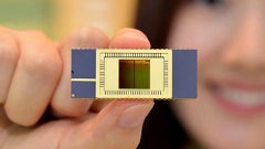
Called V-NAND, the technology layers the memory chips on top of each other, instead of side-by-side, thus saving precious space and allowing for larger capacities, not to mention faster and more durable internal storage chips. Samsung managed to stack not one or two, but 24 of those NAND modules on top of each other, and it's the interconnect between those that it says is the "secret sauce" for making the memory faster.
Not only faster, but in large capacities, too, as those V-NAND chips start you off with 16 GB of internal storage, shooting all the way up to 128 GB, thus all but eliminating the need for a separate microSD card slot, for example. The best part is that this is not some far-fetched technology years down the pipeline, but Samsung has actually sent those out for mobile device makers to sample, and is ready to produce them in mass quantities.
The V-NAND chips are expected to make it in SSD memory as soon as this year, and in mobile devices they will be landing in 2014, said Samsung, and added that the technology is a result of no less than 10 years of research on its part, now guarded by more than 300 patents.
Samsung Starts Mass Producing Industry’s First 3D Vertical NAND Flash
Samsung Electronics announced that it has begun mass producing the industry’s first three-dimensional (3D) Vertical NAND (V-NAND) flash memory, which breaks through the current scaling limit for existing NAND flash technology. Achieving gains in performance and area ratio, the new 3D V-NAND will be used for a wide range of consumer electronics and enterprise applications, including embedded NAND storage and solid state drives (SSDs).
Samsung’s new V-NAND offers a 128 gigabit (Gb) density in a single chip, utilizing the company’s proprietary vertical cell structure based on 3D Charge Trap Flash (CTF) technology and vertical interconnect process technology to link the 3D cell array. By applying both of these technologies, Samsung’s 3D V-NAND is able to provide over twice the scaling of 20nm-class* planar NAND flash.
For the past 40 years, conventional flash memory has been based on planar structures that make use of floating gates. As manufacturing process technology has proceeded to the 10nm-class* and beyond, concern for a scaling limit arose, due to the cell-to-cell interference that causes a trade-off in the reliability of NAND flash products. This also led to added development time and costs.
Samsung’s new V-NAND solves such technical challenges by achieving new levels of innovation in circuits, structure and the manufacturing process through which a vertical stacking of planar cell layers for a new 3D structure has been successfully developed. To do this, Samsung revamped its CTF architecture, which was first developed in 2006. In Samsung’s CTF-based NAND flash architecture, an electric charge is temporarily placed in a holding chamber of the non-conductive layer of flash that is composed of silicon nitride (SiN), instead of using a floating gate to prevent interference between neighboring cells.
By making this CTF layer three-dimensional, the reliability and speed of the NAND memory have improved sharply. The new 3D V-NAND shows not only an increase of a minimum of 2X to a maximum 10X higher reliability, but also twice the write performance over conventional 10nm-class floating gate NAND flash memory.
By making this CTF layer three-dimensional, the reliability and speed of the NAND memory have improved sharply. The new 3D V-NAND shows not only an increase of a minimum of 2X to a maximum 10X higher reliability, but also twice the write performance over conventional 10nm-class floating gate NAND flash memory.
Also, one of the most important technological achievements of the new Samsung V-NAND is that the company’s proprietary vertical interconnect process technology can stack as many as 24 cell layers vertically, using special etching technology that connects the layers electronically by punching holes from the highest layer to the bottom. With the new vertical structure, Samsung can enable higher density NAND flash memory products by increasing the 3D cell layers without having to continue planar scaling, which has become incredibly difficult to achieve.
After nearly 10 years of research on 3D Vertical NAND, Samsung now has more than 300 patent-pending 3D memory technologies worldwide. With the industry’s first completely functional 3D Vertical NAND memory, Samsung has strengthened its competitiveness in the memory industry as well as set the foundation for more advanced products including one terabit (Tb) NAND flash, while setting a faster pace for industry growth.
According to IHS iSuppli, the global NAND flash memory market is expected to reach approximately US $30.8 billion in revenues by the end of 2016, from approximately US $23.6 billion in 2013 with a CAGR of 11 percent, in leading growth of the entire memory industry.
source: Samsung


Things that are NOT allowed: